


OFF
Voltage Range
GO LOCAL
| Company | Stock | Price |
|---|---|---|


17 g
Status:
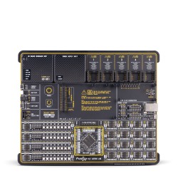
VREF Click is a compact add-on board designed to provide a stable and accurate voltage reference for low-power, noise-sensitive applications. This board features the REF34xx series from Texas Instruments, a high-precision CMOS voltage reference. Key features include ultra-low temperature drift of 6 ppm/°C, initial accuracy of ±0.05%, low power consumption under 95µA, and output noise as low as 3.8μVp-p/V. The board supports multiple voltage versions (2.5V, 3V, 3.3V, and 4.096V), with a ±10mA output current and excellent long-term stability. Thanks to the Click Snap feature, size, weight, and power consumption can be reduced for final-phase prototyping. Typical use cases include data acquisition systems, high-resolution ADC/DAC designs, and both positive and negative voltage reference applications.
VREF Click is fully compatible with the mikroBUS™ socket and can be used on any host system supporting the mikroBUS™ standard. It comes with the mikroSDK open-source libraries, offering unparalleled flexibility for evaluation and customization. What sets this Click board™ apart is the groundbreaking ClickID feature, enabling your host system to seamlessly and automatically detect and identify this add-on board, alongside a Click Snap feature introducing a new level of flexibility and ease of use.
This product is no longer in stock
Availability date: 04/20/2025
OFF
| Company | Stock | Price |
|---|---|---|
VREF Click is based on the REF34xx, a high-precision CMOS voltage reference from Texas Instruments, designed to provide a stable and accurate voltage output in low-power and noise-sensitive applications. The REF34xx features a low temperature drift of just 6 ppm/°C and an initial accuracy of ±0.05%, ensuring consistent performance across varying environmental conditions. With a power consumption of less than 95µA and an ultra-low output noise of only 3.8μVp-p/V, the VREF Click is an ideal choice for high-resolution data acquisition systems where signal integrity is crucial. VREF Click is available in multiple versions to suit different design requirements: 2.5V (REF3425), 3V (REF3430), 3.3V (REF3433), and 4.096V (REF3440), with the 2.5V version as the default configuration. The device supports an output current of ±10mA and has a maximum zero load dropout voltage of just 100mV, while offering excellent long-term stability of 25ppm over 1000 hours. Its low output-voltage hysteresis and minimal long-term drift further enhance system reliability. VREF Click is compatible with a wide range of ADC and DAC components, including the ADS1287, DAC8802, and ADS1112, and is commonly used in applications such as positive and negative voltage references and various data acquisition systems.
.jpg)
This Click board™ is designed in a unique format supporting the newly introduced MIKROE feature called "Click Snap." Unlike the standardized version of Click boards, this feature allows the main chip area to become movable by breaking the PCB, opening up many new possibilities for implementation. Thanks to the Snap feature, the REF34xx can operate autonomously by accessing their signals directly on the pins marked 1-8. Additionally, the Snap part includes a specified and fixed screw hole position, enabling users to secure the Snap board in their desired location.
VREF Click uses a single communication line - the EN (Enable) pin - to control the operational state of the REF34xx voltage reference. When the EN pin is pulled HIGH, the device enters Active mode and functions normally, delivering a precise output voltage. Pulling the EN pin LOW places the device into a low-power Shutdown mode, in which the output becomes high impedance and the quiescent current drops to just 2µA, significantly reducing power consumption. For visual indication of the device’s status, the board includes a red LED labeled LD2, which lights up when the device is enabled. If desired, this LED can be disabled by cutting the NT1 trace on the PCB, allowing for even lower power usage in energy-sensitive applications.
This Click board™ can operate with either 3.3V or 5V logic voltage levels selected via the VCC SEL jumper. This way, both 3.3V and 5V capable MCUs can use the communication lines properly. Also, this Click board™ comes equipped with a library containing easy-to-use functions and an example code that can be used as a reference for further development.
Click Snap is an innovative feature of our standardized Click add-on boards, introducing a new level of flexibility and ease of use. This feature allows for easy detachment of the main sensor area by simply snapping the PCB along designated lines, enabling various implementation possibilities. For detailed information about Click Snap, please visit the official page dedicated to this feature.
Type
Linear
Applications
Ideal for data acquisition systems, high-resolution ADC/DAC designs, and both positive and negative voltage reference applications
On-board modules
REF34xx - high-precision CMOS voltage reference from Texas Instruments
Key Features
Low temperature drift, high initial accuracy, ultra-low power consumption, low output noise, multiple fixed output voltage options, high output current capability, excellent long-term stability, low output-voltage hysteresis, high impedance shutdown mode, and more
Interface
GPIO
Feature
Click Snap,ClickID
Compatibility
mikroBUS™
Click board size
M (42.9 x 25.4 mm)
Input Voltage
3.3V or 5V
This table shows how the pinout on VREF Click corresponds to the pinout on the mikroBUS™ socket (the latter shown in the two middle columns).
| Notes | Pin | Pin | Notes | ||||
|---|---|---|---|---|---|---|---|
| NC | 1 | AN | PWM | 16 | EN | Device Enable | |
| NC | 2 | RST | INT | 15 | NC | ||
| ID COMM | CS | 3 | CS | RX | 14 | NC | |
| NC | 4 | SCK | TX | 13 | NC | ||
| NC | 5 | MISO | SCL | 12 | NC | ||
| NC | 6 | MOSI | SDA | 11 | NC | ||
| Power Supply | 3.3V | 7 | 3.3V | 5V | 10 | 5V | Power Supply |
| Ground | GND | 8 | GND | GND | 9 | GND | Ground |
| Label | Name | Default | Description |
|---|---|---|---|
| LD1 | PWR | - | Power LED Indicator |
| LD2 | LD2 | - | Device Enable LED Indicator |
| JP1 | VCC SEL | Left | Power Voltage Level Selection 3V3/5V: Left position 3V3, Right position 5V |
| Description | Min | Typ | Max | Unit |
|---|---|---|---|---|
| Supply Voltage | 3.3 | - | 5 | V |
| Output Reference Voltage | 2.5 / 3 / 3.3 / 4.096 | V | ||
VREF Click demo application is developed using the NECTO Studio, ensuring compatibility with mikroSDK's open-source libraries and tools. Designed for plug-and-play implementation and testing, the demo is fully compatible with all development, starter, and mikromedia boards featuring a mikroBUS™ socket.
Example Description
This example demonstrates the use of the VREF Click board by enabling and disabling its 2.5V reference output periodically. The application toggles the output every 3 seconds and logs the current state via UART.
Key Functions
vref_cfg_setup This function initializes Click configuration structure to initial values.vref_init This function initializes all necessary pins and peripherals used for this Click board.vref_enable_output This function enables VREF output by setting the EN pin to high logic state.vref_disable_output This function disables VREF output by setting the EN pin to low logic state.Application Init
Initializes the logger and configures the VREF Click driver.
Application Task
Alternately enables and disables the voltage reference output with a 3-second delay, displaying the output state on the UART terminal.
Application Output
This Click board can be interfaced and monitored in two ways:
Additional Notes and Information
The complete application code and a ready-to-use project are available through the NECTO Studio Package Manager for direct installation in the NECTO Studio. The application code can also be found on the MIKROE GitHub account.
NOTE: Please be advised that any peripheral devices or accessories shown connected to the Click board™ are not included in the package. Check their availability in our shop or in the YMAN section below.

$1.20

$1.74

$3.00

$1.20

$889.00

$95.00

$549.00

$299.00
$29.00
$29.00
$6.59
$3.60

$119.00
$449.00
$349.00
$349.00
$349.00

$299.00
$269.00
$249.00

$209.00
