Flash memory is the new normal, but it is a misunderstood technology when it comes to how the memory works. We are going to shed some new light on an old idea and hopefully expand your understanding of what makes for a read and write.
Introduction
When memory first arrived on the scene, a few KB of memory would cost you the same as a fine sailing ship. Today, memory has become very affordable and we use it in almost every device. The 2 types are NOR or NAND gate based with the most common today being NAND. In fact, NAND memory is found in our MCUs but an additional SPI bus controlled NAND is placed on all the mikromedia products. This is the subject of our discussion today and looking at how to use it. Of course we have provided a great library to abstract some of the complexity, but knowing how it works will make for a more effective use of the tech.
Advantages and Disadvantages
Flash memory is non-volatile, meaning that the state that it is in, remains the same when the current is removed from them. In contrast, RAM is volatile and is reset to its default state when current is removed. The advantage here goes to flash in the fact that your data doesn't disappear when the power is turned off. The disadvantage to flash initially comes in the form of performance. This is due to a couple of things, time that the charge of electrons needs to be present on the gates, and to some degree, from the limitation that flash memory has to be written to in sizes known as pages instead of a simple byte at a time. Reading flash is dramatically faster in most cases due to not having the limitation of a charge being held on the transistors for a specific time period.
| SRAM | FLASH | |
| Performance | X | |
| Cost | X | |
| Durable | X | |
| Volatile | X | |
| Power | X |
Power consumption also goes to flash. With RAM we constantly have to charge the gates with current to keep the state, but since flash is non-volatile we can write to it, then remove all power with the contents intact.
Cost can be a factor when looking at large amounts of storage. RAM is expensive to manufacture and the faster the memory, the faster your bill increases.
Durable category goes to RAM. Flash memory gets worn every time a voltage is applied to write / erase the memory. The transistors can only take so much of this before they no longer can be erased. Normal life cycle of most NAND memory is 10,000 write cycles with RAM being infinite.
Choosing A Memory Solution
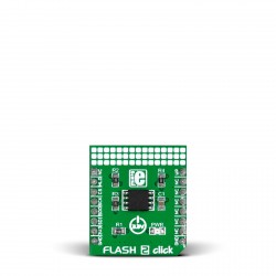
Flash memory has a few interface choices, SPI, SDIO, and I2C are among the most common. SPI is a general balance between pin count and speed, SDIO sacrifices pins for speed, and I2C gives up performance for sparing some pins. Sizes range like the color of the rainbow with most popular being in the MB size. For example, a generally good choice is the MikroElektronika Flash 2 click.

SPI based and a capacity of 8 MB of storage. With a bus frequency that can reach 75MHz, your theoretical throughput can exceed what most smaller MCUs can handle.
Blocks, Planes and Pages
 NAND Flash Die ( courtesy of AnandTech )
A flash chip is considered the "package" and contains these 4 important features.
Die is the smallest unit that can execute commands or report status.
Planes can have concurrent, or identical operations done on them with some restriction.
Blocks are the smallest unit in flash memory that can be erased at one time. ( Blocks are also known as sectors )
Pages are the units within blocks, and are the smallest unit in flash memory that can be written to.
Pages can be read from and written to by the user, but memory must be erased in blocks. In order to erase something from flash memory, you must first take into consideration the other memory inside of that block. If you want to keep that memory, you must copy it elsewhere, erase, and then place it back where it was. To prevent wearing out your flash memory very quickly, refrain from moving memory around to erase all of the time, and try to wait to erase memory until another time. A better way of writing new data to flash, is to write your new data to a different page, somehow pointing any further access to that data to the new page, and marking the old space as space to eventually be erased.
NAND or NOR
NAND and NOR memory have many different advantages and disadvantages, making one or the other more fit for a certain purpose.

NAND memory is used the most in high capacity data storage , because of its' fast write cycles, large data capacity (8MB-128MB) and long life span of over 10 times the life span of NOR memory. The price of NAND is also low, making large amounts of data storage cheaper. Typical applications using NAND memory are PC Cards, compact flash, secure digital media, and MP3 players (data only).
NOR memory is used for code storage and execution, usually in small capacities. NOR memory has code execution capabilities but very slow erase and writing cycles, making it not ideal for much more than code execution. NOR memory is also more expensive than NAND, and can hold less memory(1MB-16MB ), making it really only ideal for code storage and LOW-END embedded devices. Typical applications of NOR memory are simple home appliances, embedded designs, low-end set top boxes, low-end mobile handsets, and code storage of digital cameras.
Types of NAND Memory Cells
There are three types of flash memory cells in NAND memory, there is SLC( Single Level Cell ), MLC( Multi Level Cell ) and TLC( Three Level Cell ). These three types define the difference between read, write and erase time for your flash device.

Cells within your flash memory are usually floating gate transistors, and programming your flash memory simply filling this gate with electrons, and erasing memory would be removing electrons from the floating gate. The amount of electrons in the gate can be measured, and used to determine its' value. In the picture above, SLC can either be a 0 or a 1. If the electrons fill up less than 50% of the gate, it is a 1. If the gate is filled more than that, it is considered a 0. MLC measures electrons even closer, and is able to extract four different values from the amount of electrons in the gate, and lastly TLC measures the amount of electrons in a single gate so precisely, that it is able to get eight different values from a single gate.
As you can imagine, SLC is much quicker than MLC or TLC when it comes to reading, writing or erasing. The only advantage to measuring the electrons in the gate closer and moving from a SLC to a MLC or TLC, is cost. You can fit more memory on less gates, decreasing the price of the product. Here is a chart of the exact differences in time between these three types.

Using Flash 2 Click
The flash memory on the Flash 2 Click is organized in uniform, 4 KByte erasable sectors with the following erasable blocks: eight 8 KByte parameter, two 32 KByte overlay, and one-hundred twenty-six 64 KByte overlay blocks. Here is a graphic to show how it is layed out.

To use the flash 2 click, it is very simple. First the pins for the Write Protect, Chip Select, and Hold must be set.
sbit FLASH_2_WP at GPIOA_ODR.B0;
sbit FLASH_2_CS at GPIOD_ODR.B13;
sbit FLASH_2_HLD at GPIOC_ODR.B2;
The next step is to initialize the SPI communication bus. On the EasyMXPro V7 the SPI initialization is as follows:
SPI1_Init_Advanced( _SPI_FPCLK_DIV64,
                          _SPI_MASTER | _SPI_8_BIT | _SPI_CLK_IDLE_LOW |
                          _SPI_FIRST_CLK_EDGE_TRANSITION | _SPI_MSB_FIRST |
                          _SPI_SS_DISABLE | _SPI_SSM_ENABLE |
                          _SPI_SSI_1,
                          &_GPIO_MODULE_SPI3_PC10_11_12 );
The final steps to initialization is to call flash_2_init to initialize the HAL layer functions, and then flash_2_global_block_unlock to unlock the blocks for read, write and erase ( the small delays are just to allow full initialization of the HAL layer, and unlocking of all blocks of memory, smaller delays can be used ).
flash_2_init();
Delay_ms(300);
flash_2_global_block_unlock();
Delay_ms(300);
Now, to read or write, it takes a simple address to write/read to, a buffer/receive_buffer and a count for the amount of data you are writing/reading.
uint8_t  buffer[4]           = {15,20,25,30}; // Used for writing
uint16_t count               = 4;             // Number of bytes to read/write
uint32_t address             = 0x0100F0;      // Address to start read/write
uint8_t  receive_buffer[4]   = { 0 };         // Used for reading

flash_2_write( address, buffer, count );         //Write 4 bytes to 0x0100F0 from buffer
flash_2_read( address, receive_buffer, count );  //Read 4 bytes into receive_buffer from 0x0100F0
There are three choices for erasing. Erasing can be done by the sector, by block, or the entire chip. Sector and block take a starting address to start the erase from, and chip does not take anything, and erases the entire chip, setting all bits to 1.
void flash_2_sector_erase( uint32_t address )
void flash_2_block_erase( uint32_t address )
void flash_2_chip_erase( void )
Links to the libraries can be found at Libstock or Github.
Summary
Flash is an inexpensive and easy storage solution for the embedded world. For an easy-to-use memory for your project, Flash and Flash 2 click boards are ideal. The library is complete with write, read, erase and many more capabilities. It is also ready for use on any of the development platforms.
References
Flash Memory, wikipedia.org 2016
Understanding Flash, flashdba.com 2014
Two Flash Technologies Compared https://focus.ti.com 2002


