


One of the most popular communication protocols for communicating with clicks or other MCUs is SPI (Serial Peripheral Interface). Communication is implemented with a SPI Master and one or multiple SPI slaves. In this blog, we will talk about how SPI communication is used. For clarity, we will look at some examples of SPI communication from datasheet, to implementation in C.
Wiring
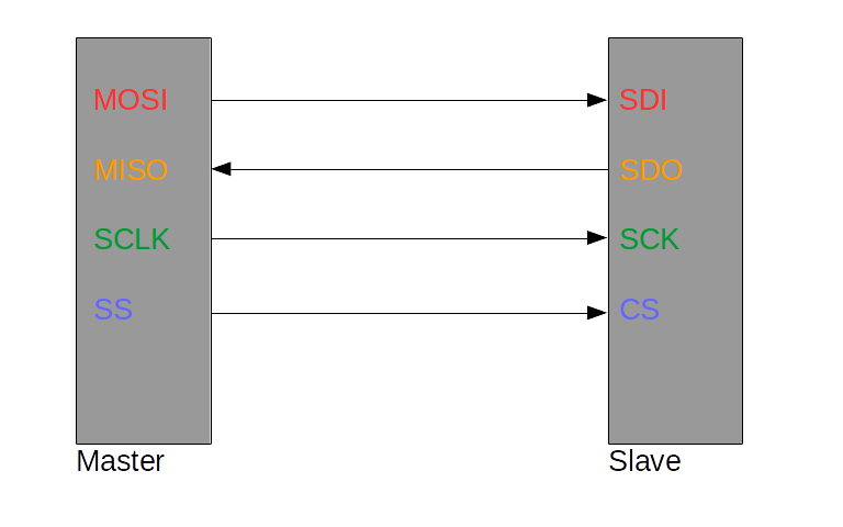
Normal SPI communication uses 4 wires.
Master:
- MISO - Master In Slave Out
- MOSI - Master Out Slave In
- SCLK - Serial Clock
- SS - Slave Select
Slave:
- SDI - Slave Data In
- SDO - Slave Data Out
- SCK - Serial Clock
- CS - Chip Select
SPI communication is a synchronous communication protocol, which means it can send out data on the MOSI line and it doesn't have to wait for a response before doing other operations. SPI is also operates at full-duplex, in other words data can be received and transmitted simultaneously.
SPI Modes
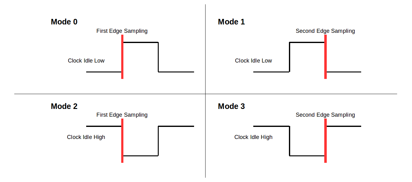
Before discussing how communication is done with wires, we must understand the 4 different modes SPI can be initialized to. At the lowest level, there is the SCLK wire which gives the slave a clock signal to use for communicating. The 4 modes are determined by the states of two things, the Clock Phase (CPHA) and Clock Polarity (CPOL). In some cases SPI libraries will use these modes to initialize SPI bus communication. In the case of MikroC, we use terms like "clock-idle low" or "clock-idle high" for clock polarities, and "first edge" or "second edge" for clock phases. Let's start with a diagram to better explain different ways of communicating through SPI.
When the clock polarity is set to low (0) and the clock phase is set to "first edge" then the mode is considered Mode 0. In this case, data is shifted onto the MOSI line when the clock rises from low (0) to high (1). In Mode 3, the clock phase is also set to shift data onto the MOSI line on the "first edge", but in this case the clock polarity is high (1), which means that the data must be shifted when the clock falls from high (1), to low (0).

Protocol
SPI uses a SS line or "Slave Select" for telling the slave when the master is going to start producing a clock signal on SCLK. This line can be set to idle high or low as well, but in most cases the chip select is held high when the master is not ready to communicate with the slave, and pulled low to initialize communication. Here is a step by step list of what normally goes on when SPI communication is happening with a peripheral:
- SPI Master pulls the SS low (in some cases high, depending on the idle state of SS)
- SPI Master starts producing clock signals on SCLK line
- SPI Master puts data onto the MOSI line on the correct "edge" of the SCLK signal
Here is a snippet from a datasheet for the SST26VF064B Flash Memory Chip used on the Flash 2 Click for communicating with the module through SPI.
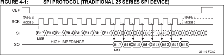
Note: If this is the first time looking at a SPI timing diagram from a datasheet take a deep breath and relax, this isn't as scary as you might think.
In this diagram, we have SPI slave pins labeled on the left. As seen in the diagram in this blog in the section on Wiring, these lines are connected from CE (CS) to SS, SCK to SCLK, SI to MOSI, and SO to MISO. In this case, CE or chip select is held high, and when pulled low, communication begins. This specific chip supports both Mode 3 or Mode 0 SPI modes and the diagram reflects such. This means that the clock can idle high or low, but the data is always taken on the first edge of the clock oscillation.
Another difference that can happen but not very often, is data being send to the slave can be MSb (Most Significant Bit) first, or LSb (Least Significant Bit) first. In this case the slave is expecting data as MSb first. In some cases, slave modules will require 16 bits of data at a time, and you will need to look at this diagram closely to determine if MSB means "Most Significant Bit" or "Most Significant Byte" (although i've never seen a 16bit SPI protocol ask for the most significant bit).
Let's take a closer look...

- Chip select was idling high, and was pulled low, so now the slave knows that the SCK line will start to oscillate, and data is to be expected on the first edge.
- SCK line has started oscillating, and the first edge has now happened. It doesn't matter if the SCK was idling high or low in this case, it only matters that the first edge is where the data must be sampled.
- Data has been sampled for an entire byte, and if the slave wants to it can put data for the Master SPI to read on the SO line, on the falling edge of the clock oscillation.
MikroC Example
To use the MikroC SPI library for this chip, here is how you would initialize the Master SPI bus on ARM...
    GPIO_Digital_Output( &GPIOD_BASE, _GPIO_PINMASK_13 );    // Set CS Pin to Output

    SPI3_Init_Advanced( _SPI_FPCLK_DIV64,                                          //SPI set for 8 bit communication, sclk idle low, first edge, msb first
                          _SPI_MASTER | _SPI_8_BIT | _SPI_CLK_IDLE_LOW |
                          _SPI_FIRST_CLK_EDGE_TRANSITION | _SPI_MSB_FIRST |
                          _SPI_SS_DISABLE | _SPI_SSM_ENABLE |
                          _SPI_SSI_1,
                          &_GPIO_MODULE_SPI3_PC10_11_12 );
First thing to do is set the pin for your chip select to output. SPI is initialized with alot of parameters on STM MCUs, in this case we set the SPI bus up for 8 bit data transfer, SCLK idle low, first edge transitions, and msb first.
You might be asking, "What's 8 bit data transfer?", well that's the amount of data the slave is expecting to receive when the Master SPI begins to communicate. When the CS is pulled low and the SCLK starts to oscillate for communication between master and slave, the data being transferred can be either 8 bit or 16 bit. This depends on what the slave is expecting to receive. When the slave expects 8 bits of data, and the user uses SPI3_Write( unsigned data_out ) , then the clock oscillates only enough for 8 bits of data 8 times), and then returns to idle. If the slave is expecting 16 bits, then this argument must be changed to _SPI_16_BIT for proper communication.
Writing
Next, let's take a look at the write function in the _hal layer of the flash_2 library.
void flash_2_hal_write( uint8_t *buffer,
                          uint16_t count )
{
    flash_2_hal_cs_low();
    while( count-- )
        write_spi_p( *buffer++ );
    flash_2_hal_cs_high();
}
Almost every peripheral that uses SPI communication will be different for reading and writing. In the case of Flash 2, writing is quite complex because there is a WP (Write Protect) pin, and multiple ways to write to flash memory, as well as blocks of addresses that you must write to at a time. For now, we will just discuss the HAL layer write function. CS is pulled low to initiate communication, and the we use our function pointer to SPI3_Write( unsigned data_out ) to shift data onto the MOSI line, while oscillating the SCLK correctly, depending on the way it was initialized. After all of the data has been sent to the slave, we tell the slave that we are finished by setting the CS to high once again.
Reading
Reading is very similar to writing, because there are multiple ways to read from the module; here will we just cover the basic HAL layer function, so that you understand what's going on at the bare metal.
void flash_2_hal_read( uint8_t *buffer,
                         uint16_t count )
{
    while( count-- )
        *buffer++ = read_spi_p( 0x00 );
}
In the case of Flash 2, the read function is called after giving the module an address through SPI_Write, and then calling this function. It is almost exactly how the write function looked, except we do not need to touch the CS at all because the communication in this case is already initialized before calling this function. To clarify, read_spi_p is a function pointer pointing to unsigned SPI3_Read( unsigned long buffer ) . All that is required is a dummy byte for clock generation and the data from the SPI slave will be placed into the return value.
Quick Tip
Logic analyzers are great tools for debugging and watching communication. Using logic analyzers allows you to see every clock oscillation, timings, and much more.
Here, you can see SPI communication happening very easily.

Summary
Now you know how to use SPI communication! The number one thing to remember when trying to communicate with any kind of peripheral or MCU through SPI bus is to read the datasheet! When attempting to initiate communication with any device, the datasheet should be your very best friend. The basics of SPI communication are laid out in this blog, and should be used as a place to start when figuring out those confusing and sometimes scary datasheet diagrams.

