


24%
OFF
GO LOCAL
| Company | Stock | Price |
|---|---|---|


MIKROE-3123
23 g
Status:
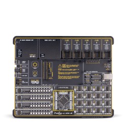
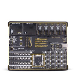
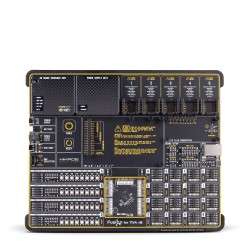
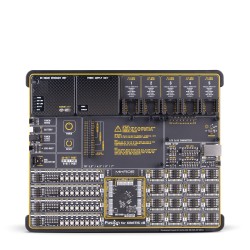
Boost-INV 2 Click is a compact add-on board that generates both positive and negative adjustable voltages for split-rail power supply applications. It is based on the TPS65131, a dual-output DC/DC converter from Texas Instruments capable of delivering regulated boost and inverting voltages from a single input source. To enable digitally controlled output voltage, the board integrates two 12-bit MCP4291 D/A converters from Microchip within the positive and negative feedback loops, supported by the MCP6H02 operational amplifier for signal inversion, the ADM8829 switched-capacitor voltage inverter, and the MCP1501 precision voltage reference. The TPS65131 operates in both continuous-conduction and power-saving modes, with low output ripple and minimal standby current consumption. This Click board™ is ideal for applications requiring dual-polarity regulated voltages such as analog signal conditioning, sensor biasing, and portable instrumentation systems.
Boost-INV 2 Click is fully compatible with the mikroBUS™ socket and can be used on any host system supporting the mikroBUS™ standard. It comes with the mikroSDK open-source libraries, offering unparalleled flexibility for evaluation and customization.
This product is no longer in stock
Availability date:
24%
OFF
| Company | Stock | Price |
|---|---|---|
Boost-INV 2 Click is based on the TPS65131, a positive and negative output DC/DC converter from Texas Instruments. This board features a set of integrated circuits which are used to achieve digitally controlled output voltage. Two D/A converters are connected into the positive and negative voltage feedback loop of the TPS65131. The positive and the negative loops are fed into the internal error amplifiers, which compare the feedback voltage with the internal references. They change the duty cycle of the output switching sections in order to compensate for the differences (errors), affecting the output voltage that way. Incorporating a D/A converter into the feedback loop allows programmed "errors" to be introduced into the loop, which in return allows control over the output voltage.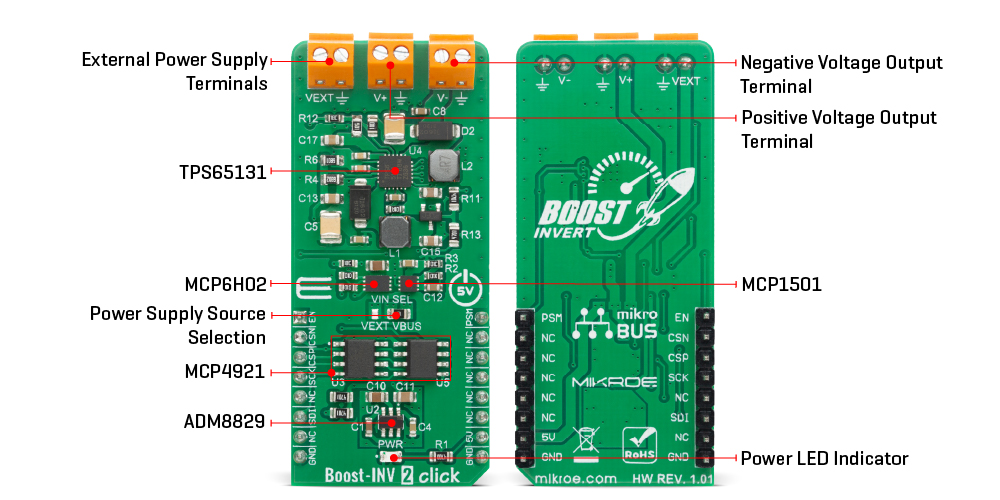
The TPS65131 uses the fixed frequency PWM signal to switch its output stages. The internal current limitation is set to about 1950mA for both the inverting and boost converter. While running in the continuous conduction mode, the output voltage is clean, with no significant ripple and noise. The complete disconnect of both inverting and boosting converter stages allows no source current flowing through the converter, while it is unpowered. This prevents battery draining, making the device able to use the battery power, providing a split-rail power supply for various applications.
Two 12-bit D/A converters, the MCP4291 from Microchip, are used in feedback loops. One of the DACs is connected to the MCP6H02 Op-Amp, configured as the inverting unity gain amplifier. It inverts the polarity of the DAC signal. The feedback voltage of the inverting converter can vary from 0V (Vref) to -15V. Therefore, the DAC signal which commonly ranges from 0 to +VREF, needs to be inverted. For the boost converter, there is no need to invert the DAC, so its voltage goes up to +VREF. There are two separate CS pins (Chip Select) for these DACs, so both can be programmed independently. Those Chip Select pins are routed to the CSN for the negative voltage controlling DAC, and CSP for the positive voltage controlling DAC. Two more auxiliary ICs are used on the Boost-INV 2 Click. One IC is the ADM8829, a switched-capacitor voltage inverter which provides a negative supply voltage for the inverting Op-Amp. The other IC is the MCP1501, a high precision buffered voltage reference required for the DACs (4.096 V).
The TPS65131 can be operated in the Power Saving mode. This is very useful for low currents because the device will power itself down as long as the voltage across the output stays above the internally set threshold. When the voltage drops under this threshold, the converter powers up and produces several switching pulses recovering the nominal voltage value across the load, and powers down again. Depending on the connected load, it will take more or less time to drain the charge from the inductor. Unlike the normal mode, which operates in the continuous-conduction mode (CCM), power saving mode allows the converter to switch between CCM and DCM (discontinuous-conduction) modes. The Click board™ has its PWM pin (PSM pin) routed to the PSP and PSN pins of the TPS65131 and HIGH logic level on this pin will put the IC into the Power Saving mode.
When the ENP and ENN pins of the TPS65131 are at the LOW logic level, the device is completely powered down, disconnecting the loads as described above, preventing current leakage through the passive elements of the circuit. These pins are routed to the EN pin of the mikroBUS™, allowing the host MCU to control the operation of the Click board™. By default, the input voltage is taken from the mikroBUS™ +5V power rail. An onboard VIN SEL jumper allows selection between the +5V from the mikroBUS™ or an external power supply connected to the screw terminal input, which is labeled as VEXT. The remaining two screw terminals are negative and positive voltage outputs, labeled as V- and V+. All three screw terminals share a common GND.
This Click board™ can be operated only with a 5V logic voltage level. The board must perform appropriate logic voltage level conversion before using MCUs with different logic levels. It also comes equipped with a library containing functions and example code that can be used as a reference for further development.
Type
Boost
Applications
Ideal for applications requiring dual-polarity regulated voltages such as analog signal conditioning, sensor biasing, and portable instrumentation systems
On-board modules
TPS65131, a positive and negative output DC/DC converter by Texas Instruments; MCP4291, a 12-Bit DACs; MCP6H02, a dual operational amplifier, MCP1501, a high precision buffered voltage reference, all by Microchip; ADM8829, a switched-capacitor voltage inverter by Analog Devices
Key Features
Programmable output positive and negative voltage up to ±15V from a single-sided low voltage, reasonably high current output, high efficiency, soft start, complete load disconnect when powered off, and more
Interface
GPIO,SPI
Feature
No ClickID
Compatibility
mikroBUS™
Click board size
L (57.15 x 25.4 mm)
Input Voltage
5V,External
This table shows how the pinout on Boost-INV 2 click corresponds to the pinout on the mikroBUS™ socket (the latter shown in the two middle columns).
| Notes | Pin | Pin | Notes | ||||
|---|---|---|---|---|---|---|---|
| Device Enable | EN | 1 | AN | PWM | 16 | PSM | Power-Save Mode Control |
| DAC Chip Select (Negative) | CSN | 2 | RST | INT | 15 | NC | |
| DAC Chip Select (Positive) | CSP | 3 | CS | RX | 14 | NC | |
| SPI Clock | SCK | 4 | SCK | TX | 13 | NC | |
| NC | 5 | MISO | SCL | 12 | NC | ||
| SPI Data IN | SDI | 6 | MOSI | SDA | 11 | NC | |
| NC | 7 | 3.3V | 5V | 10 | 5V | Power supply | |
| Ground | GND | 8 | GND | GND | 9 | GND | Ground |
| Label | Name | Default | Description |
|---|---|---|---|
| LD1 | PWR | - | Power LED indicator |
| JP1 | VIN SEL | Right | Power Supply Source Selection VEXT/VBUS: Left position VEXT, Right position VBUS |
| Description | Min | Typ | Max | Unit |
|---|---|---|---|---|
| Supply Voltage | - | 5 | - | V |
| External Power Supply Range | 2.7 | 5 | 5.5 | V |
| Positive Output Voltage (V+) | - | - | +15 | V |
| Negative Output Voltage (V-) | -15 | - | - | V |
| Output Current Limit (per converter) | - | 1950 | - | mA |
| DAC Resolution | - | 12 | - | bit |
Boost-inv 2 Click demo application is developed using the NECTO Studio, ensuring compatibility with mikroSDK's open-source libraries and tools. Designed for plug-and-play implementation and testing, the demo is fully compatible with all development, starter, and mikromedia boards featuring a mikroBUS™ socket.
Example Description
First increse positiv voltage by 2V every 3 seconda, then decrese negative value for -2v every 3 seconds.
Key Functions
boostinv2_cfg_setup Config Object Initialization function.boostinv2_init Initialization function.boostinv2_default_cfg Click Default Configuration function.boostinv2_set_positive_voltage Functions for set positive output voltage.boostinv2_set_negative_voltage Functions for set negative output voltage.boostinv2_generic_transfer Generic transfer function.Application Init
Initializes Driver init and enable chip
Application Task
Changes the positive and negative output voltage. Positive output voltage goes from 5V to 15V. Negative output voltage goes from -5V to -15V
Application Output
This Click board can be interfaced and monitored in two ways:
Additional Notes and Information
The complete application code and a ready-to-use project are available through the NECTO Studio Package Manager for direct installation in the NECTO Studio. The application code can also be found on the MIKROE GitHub account.
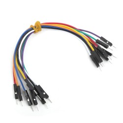
NOTE: Please be advised that any peripheral devices or accessories shown connected to the Click board™ are not included in the package. Check their availability in our shop or in the YMAN section below.

$675.64

$72.20

$417.24

$227.24
$29.00
$22.04
$5.01
$2.74

$90.44
$341.24
$265.24
$265.24
$265.24

$227.24
$204.44
$189.24

$158.84
