


Circuit boards are the backbone of modern electronics. They're found in everything from smartphones to spacecraft.
But what exactly is a circuit board?
In simple terms, a circuit board, or a printed circuit board (PCB), is a thin board made of insulating material. It's covered with conductive pathways. These pathways connect different components like resistors, capacitors, and integrated circuits.
Understanding how these boards work can seem daunting. Especially with terms like 'PCB artwork' and 'PCB layout' thrown around. But don't worry.
This guide will break down the basics of circuit boards. We'll explore their design, function, and application.
We'll also answer common questions. Like, what does a PCB do? Or, how do you design a PCB circuit board?
By the end, you'll have a solid understanding of circuit boards. Whether you're an electronics enthusiast, an engineering student, or a professional, this guide is for you.
So, let's dive into the fascinating world of circuit boards.
What is a Circuit Board?
A circuit board, commonly known as a printed circuit board (PCB), is an essential part of electronic devices. It serves as the foundation for mounting and interconnecting electronic components. These boards are present in almost every electronic device you encounter daily.
Circuit boards consist of a non-conductive base material that houses conductive paths. These paths, made from copper, connect various components to form a complete electronic circuit.
The term "PCB" stems from the manufacturing process which involves printing these conductive pathways onto the board.
The main role of a circuit board is to provide structure and support for the components. It also facilitates electrical connections between them. In this way, circuit boards enable devices to function efficiently and reliably, making them indispensable in modern electronics.
Understanding circuit boards is key to grasping how most electronic systems operate.
The Evolution of Circuit Boards
The journey of circuit boards began in the early 20th century with simple, hand-soldered connections. Initially, these boards were created manually, making them time-consuming and error-prone. This early method laid the groundwork for more advanced developments in electronics.
By the 1950s, the introduction of printed circuit technology revolutionized the industry. Conductive paths were chemically etched onto copper-clad boards, drastically improving efficiency and precision. This advancement enabled manufacturers to produce more complex and reliable electronic devices at a lower cost.
In recent years, circuit boards have seen significant technological advances. The development of multilayer and flexible PCBs has allowed for compact and complex designs. These innovations have fueled the rise of miniaturized and sophisticated electronics, including smartphones and wearable technology. Understanding these advancements highlights the pivotal role circuit boards play in modern life.
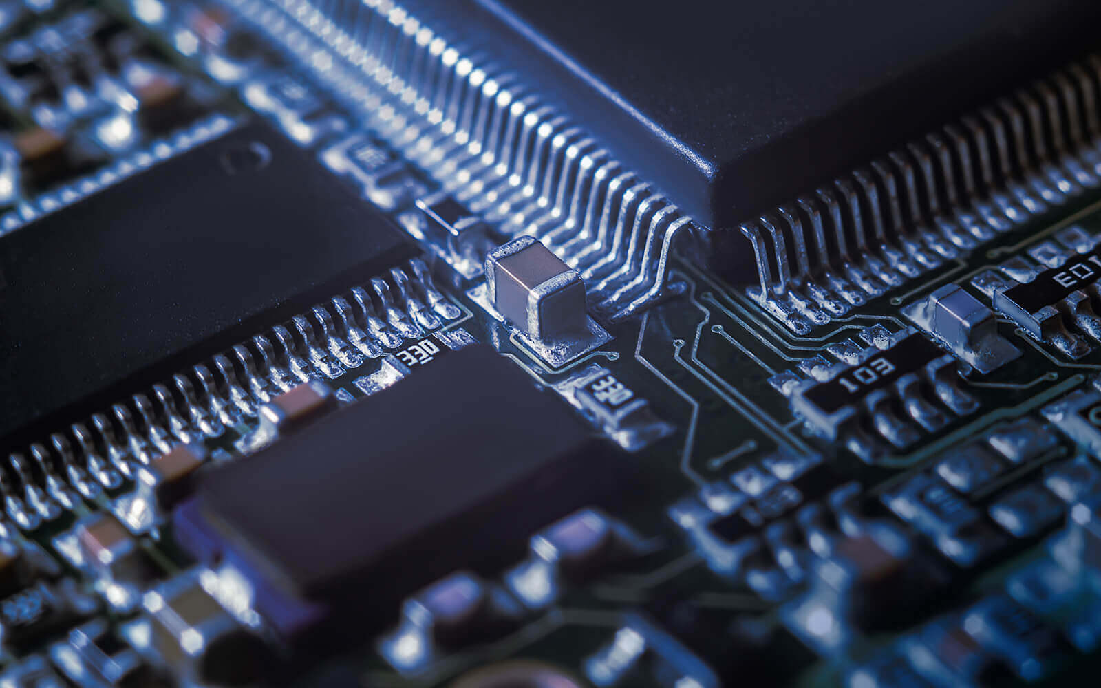
Key Components of a Circuit Board
Circuit boards are intricate puzzles made from several essential parts. Each component has a specific role, ensuring the board operates efficiently. Understanding these parts offers insight into their functions and the overall PCB design.
Traces, Pads, and Vias
Traces are like highways for electricity, connecting components on a PCB. They consist of thin lines of copper that route signals across the board. Pads act as the connection points where components are soldered onto the board.
Vias serve a critical function in enabling connections between different layers of a PCB. They are small holes filled or plated with metal, allowing electricity to flow vertically. These elements work in concert to form a functioning electrical network.
Insulating Layers and Substrates
Insulating layers are crucial in preventing electrical shorts on a circuit board. They are placed between layers of copper to isolate different parts of the circuit. Substrates provide the foundation on which components and traces are built.
Commonly used substrate materials include FR4 and CEM1. These materials offer stability and resistance to heat, which are vital for proper PCB function. Together, insulating layers and substrates ensure reliability and safety in PCBs.
Solder Masks and Silkscreens
Solder masks are protective coatings applied over the copper traces. They help prevent solder bridges during assembly and offer additional protection against environmental factors. This mask also gives the board its characteristic green color, although other colors are available.
Silkscreens are printed markings on the board, aiding in the assembly and repair process. These labels identify component locations and other important information. In combination, solder masks and silkscreens enhance both the durability and usability of PCBs.
Types of Circuit Boards
Circuit boards come in various types, each catering to specific needs and applications. Knowing the differences helps in selecting the right one for your project. PCBs are categorized based on the number of copper layers and flexibility.
Here are the main types of circuit boards:
- Single-Sided PCBs
- Double-Sided PCBs
- Multilayer PCBs
- Rigid and Flexible PCBs
Each type has its unique structure and benefits, making them suitable for different uses.
Single-Sided PCBs
Single-sided PCBs are the simplest type, containing only one copper layer. This layer supports the entire network of traces and components. They are cost-effective and ideal for straightforward electronics like calculators and radios.
However, due to limited connectivity, they're not suited for complex projects. Their simplicity makes them easier and cheaper to produce, but limits their application scope.
Double-Sided PCBs
Double-sided PCBs have copper layers on both sides of the board. This setup enhances their capability by allowing for more complex circuits. Components can be placed on both sides, connected via vias.
They provide more flexibility and are used in advanced applications like lighting systems and industrial controls. Double-sided PCBs strike a balance between complexity and affordability.
Multilayer PCBs
Multilayer PCBs consist of multiple copper layers interleaved with insulating material. These layers are bonded together, forming a compact and powerful board. They support very complex circuits found in high-tech devices.
They enable the compact design of tablets, smartphones, and other space-constrained gadgets. Their complexity allows designers to pack more functionality into smaller spaces.
Rigid vs. Flexible PCBs
Rigid PCBs maintain a solid structure and are unable to bend. They're used in applications where durability and reliability are essential, such as desktop computers.
Flexible PCBs are made from flexible plastic substrates, allowing them to bend and fold. They're perfect for wearable technology and devices with limited space. Each type offers unique advantages tailored to specific electronic needs.
How Do Circuit Boards Work?
Understanding how circuit boards function is crucial for electronics enthusiasts and professionals alike. Circuit boards serve as the backbone of electronic devices. They connect and organize components, enabling them to work together effectively.
A circuit board primarily guides electric currents through the layout of copper traces. It acts as the medium that holds components in place. This enables the flow of electricity between them without direct contact.
Components like resistors, capacitors, and chips are soldered onto the board. The circuit board connects them using pathways etched in copper. These connections are vital for the control and distribution of electrical signals.
Here's what circuit boards achieve:
- Ensure proper alignment and connectivity of components.
- Facilitate signal and power distribution across the circuit.
- Isolate sections to prevent short circuits.
Without circuit boards, assembling electronic circuits would be chaotic and unreliable. Their design is crucial for both performance and efficiency.
The Role of Copper Traces
Copper traces are the unsung heroes of a PCB. They form the intricate pathways on which signals travel. These traces replace wires to connect components, maintaining a neat and compact form.
The width and thickness of these traces are crucial. They affect the amount of current that can safely pass through. Properly designed copper traces prevent overheating and ensure signal integrity.
Traces must be carefully routed to avoid interference. Efficient routing ensures the signals reach their destination quickly. Attention to detail is essential, especially in high-frequency designs.
The Importance of Proper Layout
The layout of a circuit board can make or break its functionality. A well-thought-out layout ensures reliability and reduces potential errors. Proper spacing and organization help prevent unwanted interactions and shorts.
Designing a PCB layout involves planning component placement with care. Components should be arranged to minimize trace lengths. This aids in reducing resistance and improving overall performance.
Additionally, a good layout simplifies troubleshooting and modifications. Proper design foresight helps in managing future updates or repairs. The effectiveness of the entire device depends heavily on the layout of the circuit board.
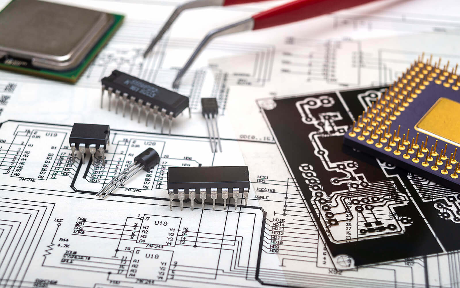
Designing a PCB: From Schematic to Layout
Designing a printed circuit board (PCB) involves several key stages, beginning with the creation of a schematic. This schematic serves as the blueprint for your circuit, detailing how components are interconnected. Utilizing a schematic streamlines the design process, as it visually maps out the entire circuit.
Once the schematic is ready, translating it into an actual layout is the next step. This involves plotting the physical placement of components on the board. The layout must consider space, trace routes, and heat management to optimize functionality.
It's important to ensure that the design adheres to industry standards. Compliance not only ensures reliability but also facilitates easier manufacturing and testing. One critical aspect is the efficient use of space to minimize board size without compromising performance.
During the layout phase, designers often face challenges such as balancing performance with manufacturability. It's crucial to avoid overcrowding components, which can lead to overheating or interference. Design tools and simulations help in identifying potential issues early.
Here are the typical steps in PCB design:
- Create the circuit schematic.
- Convert schematic to layout.
- Optimize component placement.
- Route the connections (traces).
- Conduct design checks for errors.
Finally, having a well-thought-out design can significantly reduce costs and production time. It also makes maintenance and troubleshooting easier in the long run.
PCB Design Software Tools
Designing a PCB requires the right tools to convert electronic ideas into tangible products. Software tools simplify this process, offering powerful features for both schematics and layouts. Popular PCB design tools like Eagle, Altium Designer, and KiCad are highly recommended.
Each tool has its strengths, catering to different user needs and expertise levels. Eagle is known for its user-friendly interface, making it ideal for beginners. Altium Designer offers advanced features suitable for complex projects, while KiCad is an open-source tool praised for its versatility.
These software tools come equipped with libraries of components. Designers can drag and drop parts into their schematics or layouts. This saves valuable time and ensures accuracy in design specifications.
Choosing the right software can greatly impact your project’s success. Factors such as cost, usability, and community support are worth considering. It’s essential to select a tool that aligns with your project needs and skill level.
Prototyping and Testing
After finalizing the PCB layout, prototyping becomes the next logical step. Prototyping involves creating a preliminary version of your PCB to test its functionality. This stage is vital in identifying design flaws before full-scale production.
Prototypes allow designers to simulate real-world usage. They can verify whether the circuit operates as intended under various conditions. This helps in adjusting the design for performance enhancements or error fixes.
Testing is an integral part of prototyping. It involves subjecting the PCB to rigorous assessments to ensure reliability. Issues like signal interference, current flow, and heat dissipation are scrutinized during testing.
Thorough testing reduces the risk of failure in the final product. It provides valuable insights, contributing to refining the design even further. Overall, the prototyping and testing phase is essential for achieving a robust and efficient PCB design.
PCB Fabrication and Assembly
The journey from a PCB design to a physical board involves fabrication and assembly.
Fabrication is where the blueprint comes to life through precise techniques. The process ensures the board meets the required specifications and standards.
Modern fabrication combines traditional methods with cutting-edge technology. This integration enhances precision and efficiency. Skilled technicians and sophisticated machinery play pivotal roles.
Assembly follows fabrication and involves attaching components. It's a meticulous process requiring attention to detail. Assembling ensures components are correctly positioned and securely fixed.
With advancements in technology, assembly has become faster and more reliable. Automation is prevalent, reducing human error and speeding up production. The use of robots for soldering is a common practice in modern PCB assembly.
Here are the typical steps involved in the PCB process:
- Design review and preparation of the Gerber file.
- Production of photomasks for patterning traces.
- Etching to remove unnecessary copper.
- Drilling of holes for components.
- Application of solder masks and silkscreen.
Both fabrication and assembly demand strict quality control. Testing at every stage ensures functionality and longevity. Rigorous checks prevent defects that could affect the final product.
Fabrication Process Steps
Fabrication begins with the transfer of PCB layout onto copper-clad laminate sheets. This step involves generating a photomask from the layout file. The mask shields areas from etching solutions, forming trace patterns.
Etching removes unwanted copper, revealing the circuit paths that connect components. The precision of this step ensures no short circuits occur on the board. Various etching techniques, including chemical and laser, are employed.
Once etching is done, holes are drilled to accommodate component leads and vias. Drilling requires high precision to maintain the integrity of the board. After drilling, layers are laminated to form a stable, insulated structure.
A solder mask is then applied, providing protection against oxidation and shorts. Finally, a silkscreen layer adds labels for components and guides for assembly. This completes the board and prepares it for assembly.
Assembly Techniques: SMT and THT
In PCB assembly, components are affixed using Surface Mount Technology (SMT) or Through-Hole Technology (THT). Each method has its specific applications and benefits.
SMT is a modern approach where components are placed directly onto the board’s surface.
This technique suits compact designs, enhancing miniaturization. SMT allows for high-density assembly and faster production cycles.
Conversely, THT involves inserting component leads through drilled holes. This method excels in providing mechanical strength to components. THT is favored in applications where reliability under stress is crucial.
Both techniques often coexist in hybrid assemblies. This blending maximizes the advantages of each method. Such assemblies are adaptable, serving diverse electronic requirements.
Each technique undergoes inspection to verify connections. Proper technique selection impacts the board's performance and durability. Thus, knowing when to use SMT or THT is essential for a successful assembly process.
Common PCB Issues and Troubleshooting
PCBs are fundamental to electronic devices, but they aren't immune to issues. Problems often arise during design, fabrication, or usage. Troubleshooting these issues is crucial for maintaining device reliability.
Most common problems include short circuits, open circuits, and overheating. Each issue can cause malfunction and affect device performance. Identifying the root cause is the first step in troubleshooting.
Engineers use various techniques to diagnose and resolve PCB problems. Visual inspections are often followed by electrical testing. Precise diagnostic tools, like oscilloscopes, help pinpoint defects.
Fixing PCB issues demands a thorough understanding of the board's design and function. Proper maintenance and regular testing can prevent future occurrences. These practices ensure longer life and optimal functioning of the PCB.
Short Circuits and Open Circuits
Short circuits occur when conductive paths unintentionally connect. They lead to current flowing in unintended areas, causing malfunctions. Short circuits often result from design errors or manufacturing defects.
In contrast, open circuits break the flow of electricity. They happen when connections are incomplete or broken. Open circuits can arise from faulty soldering or physical damage.
Both issues require careful diagnosis and resolution. Technicians locate these problems using multimeters and visual inspections. Corrective measures might include redesigning traces or repairing connections.
Overheating and Component Failure
Overheating in PCBs stems from excessive current or poor heat management. It can lead to component degradation or failure. Malfunctioning components will disrupt device operations and reliability.
Identifying hot spots on the board is essential to resolving overheating issues. Engineers use thermal imaging to track heat distribution. Efficient design practices can reduce overheating risks.
Component failure may also result from manufacturing flaws or stress. Regular inspections and tests help ensure components are functioning correctly. Addressing overheating and component failures promptly avoids larger issues later.
The Future of PCBs and Emerging Technologies
The landscape of PCBs is shifting with rapid technological advancements. Emerging technologies are setting new standards in PCB design. These changes affect how PCBs are manufactured and utilized.
Flexible PCBs are among the most groundbreaking innovations. They allow for greater design versatility and application in new fields. Flexible boards can bend and twist without breaking, unlike traditional rigid PCBs.
Embedded components are pushing the boundaries of PCB capabilities. Integrating components into the board reduces size and enhances performance. This innovation supports the demand for smaller, more efficient devices.
As technology evolves, environmental concerns become more pressing. Environmentally friendly production methods and materials are essential. Adhering to regulations like RoHS promotes sustainability in the electronics industry.
Flexible PCBs and Embedded Components
Flexible PCBs offer remarkable adaptability for various electronic applications. They are crucial for modern devices requiring unique shapes and movements. The automotive and wearable tech industries significantly benefit from flexible PCBs.
Embedded components help in minimizing device footprints. They eliminate the need for additional space for components on the board's surface. This development is crucial for advancing miniaturization in electronics.
Environmental Considerations and RoHS Compliance
The focus on environmentally friendly production is escalating. Sustainable materials and processes reduce the environmental impact of PCBs. RoHS compliance ensures hazardous substances are minimized in electronics.
Conforming to these standards is not only a legal mandate but a corporate responsibility. Eco-friendly PCBs signify a commitment to future sustainability. They protect the environment while maintaining product reliability and efficiency.
FAQs About Circuit Boards
Circuit boards are central to modern electronics, yet they can often seem complex. In this FAQ section, we break down some common questions. The aim is to enhance understanding of PCBs and their functionalities.
What Does a PCB Do in Electronics?
A PCB serves as the backbone for electronics, connecting components. It effectively carries electrical signals to ensure device functionality. Without it, most modern devices wouldn't operate.
How Long Do PCBs Last?
PCBs are designed for durability and can last many years. Their lifespan depends on environmental factors and usage conditions. Proper maintenance can extend their operational life.
Can PCBs Be Repaired?
Yes, PCBs can often be repaired depending on the damage. Minor issues like broken traces can be fixed easily. However, more severe damage might require board replacement.
How Are PCBs Made Environmentally Friendly?
PCBs become environmentally friendly through sustainable design and production. Using lead-free solder and recyclable materials helps. RoHS compliance also ensures reduced harmful substances.
What Determines PCB Thickness?
PCB thickness is determined by design requirements and application. It can affect electrical performance and mechanical strength. The material used and number of layers also play a role.
Embedded Systems in Action: 8th Gen Development Boards & MCU Cards
When discussing PCB layout and hardware design, it's impossible not to mention the latest evolution of our products – proudly named the 8th generation of hardware perfection. These boards are the result of 20+ years of investment in engineering time-saving embedded tools, featuring a clean and elegant design where every detail is thoughtfully crafted. Beyond their ergonomic form, they are also fully customizable, making them the perfect foundation for launching any new project.
Instead of starting from scratch, engineers get everything they need right out of the box – saving time and streamlining development. Special attention should be given to our boards with the SiBRAIN socket, which adds a new level of modularity and universality, essentially turning the board into a blank canvas ready to become whatever you imagine.
8th generation development boards
Find them all here
 UNI-DS v8
 EasyAVR PRO v8
 Fusion for TIVA v8
 Fusion for KINETIS v8
 Fusion for ARM v8
 Fusion for STM32 v8 with STM32F407ZG
 Fusion for PIC32 v8 with PIC32MX795F512L
 Fusion for PIC v8 with PIC18F97J94
8th generation MCU Cards
Find them all here
 SiBRAIN for PIC18F56K42
 MCU CARD 10 for PIC PIC18F65K40
 SiBRAIN for PIC24HJ256GP610
 SiBRAIN for dsPIC33EP512MU814
 SiBRAIN for PIC32MZ1024EFE144
 SiBRAIN for Kinetis MKV46F256VLH16
 SiBRAIN for AVR128DA64
 SiBRAIN for GD32VF103VBT6
Ready to take your next project to the next level? Start building with 8th generation development boards and MCU Cards – where performance meets flexibility.


 MCU CARD 11 for PIC PIC18F56K42")
 MCU CARD 10 for PIC PIC18F65K40")


 MCU CARD 5 for Kinetis MKV46F256VLH16")
 SiBRAIN for AVR128DA64")
