


The embedded world is a world of bits and bytes. To a web developer, one byte doesn't mean much, let alone one bit. It doesn't change anything drastically, and he/she doesn't raise any questions or concerns about it. For an embedded programmer, things are much, much different. If he/she is writing firmware for a slave device which registers are 8-bit, one bit can change the whole outcome, and as we said before: bugs in embedded applications can have serious consequences. That is why, when we are doing debugging, we always check and verify the values of these bytes, over and over again, until we are sure that what we are writing/reading is correct.
One of the commonly used technologies which heavily relies on the byte value sent to it is shift registers. Shift registers are usually used as an attachment to the output of a microprocessor, as pulse extenders, they were used for number addition in early computers, or for multiplying/dividing a number by 2.
In this article we will briefly cover the logic behind a shift register, and give an example of programming a shift register on our Rotary Click.
What is a shift register?
Flip Flops

In order to fully understand shift registers, we first have to understand what flip flops are (no, not the sandals, we are talking about electronics here). Flip flops are bi-stable circuits, bi-stable means that it can be in two different stable states, these states are what we recognize as 0 or 1, or better put, the presence of electricity, or it's absence. Sounds familiar, right? Every flip flop circuit can represent one bit, since it holds a value of 1 or 0. Flip flop circuits usually have one or multiple inputs, while having one or two outputs. When voltage is applied to one of the inputs, the output is changed based on the logic and the current state of the circuit. Flip flops are a fundamental part in the basic operations of computer systems.
Flip flops are divided into simple and clocked ones. Simple flip flops, or latches, are level-sensitive, meaning that their output changes with the level change. Clocked flip flops change their output on a single type of clock edge.
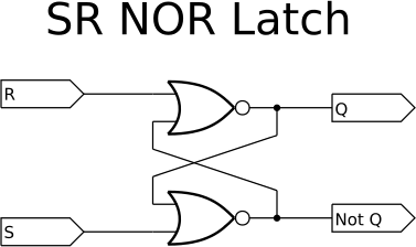
One of the most common flip flop circuits is the simple set-reset latch. This latch constitutes of a pair of cross couple NOR(negative - OR) logic gates. The S and R represent set and reset. The stored bit is represented on Q, while not-Q contains it's complementary value. Voltage brought on the S input will result in a high value on the Q output, and will stay that way until voltage is applied on R input, which will change the output to Q = 0 and NOT-Q = 1.
Now that we've understood what flip flops are, we can move on to shift registers.
A shift register is a series of flip flops connected in the way that the output of one flip flop is the input of the next one. The consequence of this type of wiring is that every bit brought on the input shifts the values of the next flip flop by 1, and the last bit on the last flip flop is lost.
Data input
Shift registers can have serial or parallel data inputs. Usually when talking about shift registers we talk SIPO (Serial in parallel out) and PISO (parallel in and serial out), although there are also SISO and PIPO configurations.
The shift register on our Rotary click is a latched SIPO register. Which means that it has an internal buffer register in which the value is stored, then when receiving a load signal (latch), the value is loaded in it's output registers.
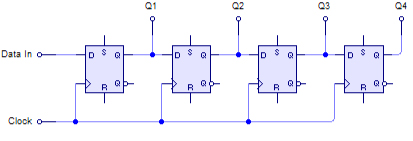 SIPO wiring of flip flop circuits
Let's look at the schematic of our Rotary click, it has two shift registers connected. The connection is simple: one 74HC595 shift register has one serial input (DS) one serial output (Q7S) and several parallel outputs, the serial output of the first shift register is connected to the serial input of the second one, so when we send a new byte to the first shift register, it will first shift whatever is stored in it to the next shift register, then receive the new value.
 Rotary click schematic displaying the wiring of two shift registers
Each bit of the stored byte in the shift register corresponds with one of the shift registers parallel outputs (q0 - q7), these outputs are connected to the LEDs, so if, for example, the register contains the value 01010101, every second LED will be lit.
Implement it in code
Let us look at a simple example of controlling multiple shift registers:
First, we need to map the required latch pin, which will initiate the transfer from the inner buffer towards the value holding register.
sbit HC595_LATCH at RE0_bit;        // map the latch pin
sbit HC595_LATCH_DIR at TRISE0_bit; // map the latch pin direction register
Now let's make a function for sending a 16-bit value to our click. Since we have two registers, we need 2 bytes (16 bits) to send to our slave device which will control our 16 pins. The important part is to remember that the first byte sent will be at the last shift register. Since it works like that, we need to send the MSB first, then the LSB. Follow the comments in the function to see how it works.
void HC595_Write_16 (uint16_t value)
{
  uint8_t first_byte, second_byte;

  second_byte = (uint8_t) value; // casting our 16-bit value to a 8bit will leave us with the LSB, we store the LSB as the second byte to be sent
  value = value>>8;              // then we shift the MSB over to the place where the LSB was, now we have an 8bit value of our MSB
  first_byte = value;            // and we store that as our first byte to be sent

  SPI1_write(first_byte);        // when the first byte is sent, it will be stored in the FIRST shift register
  SPI1_write(second_byte);       // now when we send the second byte, it will SHIFT the fist value over to the SECOND shift register
                                 // and store the second byte in the FIRST shift register

  HC595_cs = 0;                  // now it is time to pull the latch, this will transfer the values from the storage register to the value register
  asm{nop};
  asm{nop};
  asm{nop};
  HC595_cs = 1;
}
The main function will now be pretty straightforward: we configure the pins, initialize SPI protocol, and then send whatever values we want, and the function will also take care of the latching.
void main() {
  uint16_t led_state = 0x00001;   // initial value which we will send
  HC595_LATCH_DIR = 0;            // Configure latch pin as output

  SPI1_Init();                    // Initialize SPI1

  while(1)
  {
	HC595_Write_16(Led_State);
	led_state = led_state << 1;  // the dot on the led display will change position every 1 second
        if (led_state == 0)          // if the value has been shifted out to 0, set it back to 1
  		led_state = 1;
   	delay_ms(1000);
  }
}
The useful thing with shift registers is that we now have control over 16 pins just using 3 pins of our MCU. You can make your pin count even bigger, nothing is stopping you from connecting 4 shift registers and having 32 pins at your disposal!
Use the shift registers wisely, watch for the bit value, watch which bytes are being sent over your communication bus, and take full control of your surroundings!
You can also download our examples from Libstock.


