3.2 Core SFRS
The following text describes the core SFRs of the PIC16F887 microcontroller. Bits of each of these registers control different circuits within the chip, so that it is not possible to classify them in some special groups. For this reason, they are described along with the processes they are in control of.
STATUS Register
The STATUS register contains: the arithmetic status of data in the W register, the RESET status and the bank select bits for data memory.
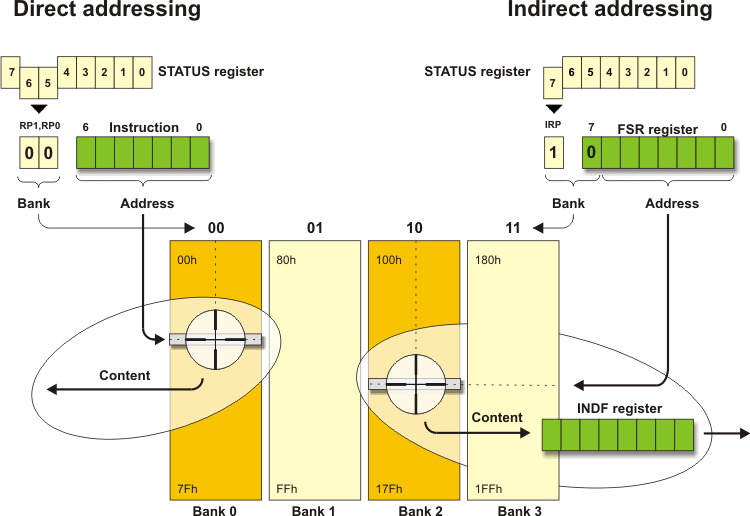
- IRP - Bit selects register bank. It is used for indirect addressing.
- 1 - Banks 0 and 1 are active (memory locations 00h-FFh)
- 0 - Banks 2 and 3 are active (memory locations 100h-1FFh)
- RP1,RP0 - Bits select register bank. They are used for direct addressing.
| RP1 |
RP0 |
ACTIVE BANK |
| 0 |
0 |
Bank0 |
| 0 |
1 |
Bank1 |
| 1 |
0 |
Bank2 |
| 1 |
1 |
Bank3 |
- TO - Time-out bit.
- 1 - After power-on, after executing the
CLRWDT instruction which resets the watch-dog timer or the SLEEP instruction which sets the microcontroller into low-consumption mode.
- 0 - After watch-dog timer time-out has occurred.
- PD - Power-down bit.
- 1 - After power-on or after executing the
CLRWDT instruction which resets the watchdog timer.
- 0 - After executing the
SLEEP instruction which sets the microcontroller into low-consumption mode.
- Z - Zero bit
- 1 - The result of an arithmetic or logic operation is zero.
- 0 - The result of an arithmetic or logic operation is different from zero.
- DC - Digit carry/borrow bit is changed during addition and subtraction if an ‘overflow’ or a ‘borrow’ of the result occurs.
- 1 - A carry-out from the 4th low-order bit of the result has occurred.
- 0 - No carry-out from the 4th low-order bit of the result has occurred.
- C - Carry/Borrow bit is changed during addition and subtraction if an ‘overflow’ or a ‘borrow’ of the result occurs, i.e. if the result is greater than 255 or less than 0.
- 1 - A carry-out from the most significant bit (MSB) of the result has occurred.
- 0 - No carry-out from the most significant bit (MSB) of the result has occurred.
OPTION_REG Register
 Legend: R/W - Readable/Writable Bit, (1) After reset, bit is set
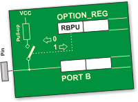
The OPTION_REG register contains various control bits to configure Timer0/WDT prescaler, timer TMR0, external interrupt and pull-ups on PORTB.
- RBPU - Port B Pull up Enable bit.
- 1 - PortB pull-ups are disabled.
- 0 - PortB pull-ups are enabled.
- INTEDG - Interrupt Edge Select bit.
- 1 - Interrupt on rising edge of RB0/INT pin.
- 0 - Interrupt on falling edge of RB0/INT pin.
- T0CS - TMR0 Clock Source Select bit.
- 1 - Transition on TOCKI pin.
- 0 - Internal instruction cycle clock (Fosc/4).
- T0SE - TMR0 Source Edge Select bit selects pulse edge (rising or falling) counted by the timer TMR0 through the RA4/T0CKI pin.
- 1 - Increment on high-to-low transition on TOCKI pin.
- 0 - Increment on low-to-high transition on TOCKI pin.
- PSA - Prescaler Assignment bit assigns prescaler (only one exists) to the timer or watchdog timer.
- 1 - Prescaler is assigned to the WDT.
- 0 - Prescaler is assigned to the TMR0.
PS2, PS1, PS0 Prescaler Rate Select bits
Prescaler rate is selected by combining these three bits. As shown in the table below, prescaler rate depends on whether prescaler is assigned to the timer (TMR0) or watch-dog timer (WDT).
| PS2 |
PS1 |
PS0 |
TMR0 |
WDT |
| 0 |
0 |
0 |
1:2 |
1:1 |
| 0 |
0 |
1 |
1:4 |
1:2 |
| 0 |
1 |
0 |
1:8 |
1:4 |
| 0 |
1 |
1 |
1:16 |
1:8 |
| 1 |
0 |
1 |
1:64 |
1:32 |
| 1 |
1 |
0 |
1:128 |
1:64 |
| 1 |
1 |
1 |
1:256 |
1:128 |
In order to achieve 1:1 prescaler rate when the timer TMR0 counts up pulses, the prescaler should be assigned to the WDT. As a result, the timer TMR0 does not use the prescaler, but directly counts pulses generated by the oscillator, which was the objective.
Let's do it in mikroC...
/* If the CLRWDT command is not executed, WDT will reset the microcontroller
   every 32.768 uS (f = 4 MHz) */

void main() {
    OPTION_REG = 0b00001111; // Prescaler is assigned to WDT (1:128)

    asm CLRWDT;              // Assembly command to reset WDT
    ...
    ...                      // Time between these two CLRWDT commands must not
    ...                      // exceed 32.768 microseconds (128x256)

    asm CLRWDT;              // Assembly command to reset WDT
    ...
    ...                      // Time between these two CLRWDT commands must not
    ...                      // exceed 32.768 microseconds (128x256)

    asm CLRWDT;              // Assembly command to reset WDT
    ...
INTERRUPT SYSTEM REGISTERS
When an interrupt request arrives, it doesn’t mean that an interrupt will automatically occur, because it must also be enabled by the user (from within the program). Because of this, there are special bits used to enable or disable interrupts. It is easy to recognize them by the letters IE contained in their names (stands for
Interrupt Enable). Besides, each interrupt is associated with another bit called the flag which indicates that an interrupt request has arrived regardless of whether it is enabled or not. They are also easily recognizable by the last two letters contained in their names- IF (
Interrupt Flag).
As seen, everything is based on a simple and efficient idea. When an interrupt request arrives, the flag bit is set first.
If the appropriate IE bit is not set (0), this condition will be completely ignored. Otherwise, an interrupt occurs! If several interrupt sources are enabled, it is necessary to detect the active one before the interrupt routine starts execution. Source detection is performed by checking flag bits.
It is important to know that the flag bits are not automatically cleared, but by software while the interrupt routine execution is in progress. If we neglect this detail, another interrupt will occur immediately after returning to the main program, even though there are no more requests for its execution. Simply put, the flag, as well as the IE bit, remain set.
All interrupt sources typical of the PIC16F887 microcontroller are shown on the next page. Note several things:
The
GIE bit enables all unmasked interrupts and disables all interrupts simultaneously.
The
PEIE bit enables all unmasked peripheral interrupts and disables all peripheral interrupts. This doesn’t concern Timer TMR0 and PORTB interrupt sources.
To enable an interrupt caused by changing logic state on PORTB, it is necessary to enable it for each bit separately. In this case, bits of the
IOCB register act as control IE bits.
INTCON Register
The INTCON register contains various enable and flag bits for TMR0 register overflow, PORTB change and external INT pin interrupts.

Legend: R/W - Readable/Writable Bit, (0) After reset, bit is cleared, (X) After reset, bit is unknown
- GIE - Global Interrupt Enable bit - controls all possible interrupt sources simultaneously.
- 1 - Enables all unmasked interrupts.
- 0 - Disables all interrupts.
- PEIE - Peripheral Interrupt Enable bit acts similar to the GIE it, but controls interrupts enabled by peripherals. It means that it has no impact on interrupts triggered by the timer TMR0 or by changing the state of PORTB or the RB0/INT pin.
- 1 - Enables all unmasked peripheral interrupts.
- 0 - Disables all peripheral interrupts.
- T0IE - TMR0 Overflow Interrupt Enable bit controls interrupt enabled by TMR0 overflow.
- 1 - Enables the TMR0 interrupt.
- 0 - Disables the TMR0 interrupt.
- INTE - RB0/INT External Interrupt Enable bit controls interrupt caused by changing the logic state of the RB0/INT input pin (external interrupt).
- 1 - Enables the INT external interrupt.
- 0 - Disables the INT external interrupt.
- RBIE - RB Port Change Interrupt Enable bit. When configured as inputs, PORTB pins may cause an interrupt by changing their logic state (no matter whether it is high-to-low transition or vice versa, the fact that something is changed only matters). This bit determines whether an interrupt is to occur or not.
- 1 - Enables the port B change interrupt.
- 0 - Disables the port B change interrupt.
- T0IF - TMR0 Overflow Interrupt Flag bit registers the timer TMR0 register overflow, when counting starts at zero.
- 1 - TMR0 register has overflowed (bit must be cleared from within the software).
- 0 - TMR0 register has not overflowed.
- INTF - RB0/INT External Interrupt Flag bit registers the change of the RB0/INT pin logic state.
- 1 - The INT external interrupt has occurred (must be cleared from within the software).
- 0 - The INT external interrupt has not occurred.
- RBIF - RB Port Change Interrupt Flag bit registers any change of logic state of some PORTB input pins.
- 1 - At least one of the PORTB general purpose I/O pins has changed state. Upon reading PORTB, the RBIF bit must be cleared from within the software.
- 0 - None of the PORTB general purpose I/O pins has changed the state.
Let's do it in mikroC...
// The PORTB.4 pin is configured as an input sensitive to logic state change

void initMain() {

ANSEL = ANSELH = 0; // All I/O pins are configured as digital
PORTB = 0;          // All PORTB pins are cleared
TRISB = 0b00010000; // All PORTB pins except PORTB.4 are configured as outputs
RBIE = 1;           // Interrupts on PORTB change are enabled
IOCB4 = 1;          // Interrupt on PORTB pin4 change is enabled
GIE = 1;            // Global interrupt is enabled
...
...                 // From this point, any change of the PORTB.4 pin logic state
                    // will cause an interrupt
...
PIE1 Register
The PIE1 register contains peripheral interrupt enable bits.

Legend: (-) Unimplemented bit, (R/W) - Readable/Writable Bit, (0) After reset, bit is cleared
- ADIE - A/D Converter Interrupt Enable bit.
- 1 - Enables the ADC interrupt.
- 0 - Disables the ADC interrupt.
- RCIE - EUSART Receive Interrupt Enable bit.
- 1 - Enables the EUSART receive interrupt.
- 0 - Disables the EUSART receive interrupt.
- TXIE - EUSART Transmit Interrupt Enable bit.
- 1 - Enables the EUSART transmit interrupt.
- 0 - Disables the EUSART transmit interrupt.
- SSPIE - Master Synchronous Serial Port (MSSP) Interrupt Enable bit - enables an interrupt request to be generated upon each data transmission via synchronous serial communication module (SPI or I2C mode).
- 1 - Enables the MSSP interrupt.
- 0 - Disables the MSSP interrupt.
- CCP1IE - CCP1 Interrupt Enable bit enables an interrupt request to be generated in CCP1 module used for PWM signal processing.
- 1 - Enables the CCP1 interrupt.
- 0 - Disables the CCP1 interrupt.
- TMR2IE - TMR2 to PR2 Match Interrupt Enable bit
- 1 - Enables the TMR2 to PR2 match interrupt.
- 0 - Disables the TMR2 to PR2 match interrupt.
- TMR1IE - TMR1 Overflow Interrupt Enable bit enables an interrupt request to be generated upon each timer TMR1 register overflow, i.e. when the counting starts from zero.
- 1 - Enables the TMR1 overflow interrupt.
- 0 - Disables the TMR1 overflow interrupt.
Let's do it in mikroC...
/* Each overflow in the Timer1 register consisting of TMR1H and TMR1L, causes an interrupt
to occur. In every interrupt rutine, variable cnt will be incremented by 1. */

unsigned short cnt;     // Define variable cnt

void interrupt() {
    cnt++ ;             // Interrupt causes cnt to be incremented by 1
    PIR1.TMR1IF = 0;    // Reset bit TMR1IF
    TMR1H = 0x80;       // TMR1H and TMR1L timer registers are returned
    TMR1L = 0x00;       // their initial values
}

void main() {
    ANSEL = ANSELH = 0; // All I/O pins are configured as digital
    T1CON = 1;          // Turn on timer TMR1
    PIR1.TMR1IF = 0;    // Reset the TMR1IF bit
    TMR1H = 0x80;       // Set initial value for timer TMR1
    TMR1L = 0x00;
    PIE1.TMR1IE = 1;    // Enable an interrupt on overflow
    cnt = 0;            // Reset variable cnt
    INTCON = 0xC0;      // Enable interrupt (bits GIE and PEIE)
    ...
PIE2 Register
The PIE2 Register also contains various interrupt enable bits.

Legend: (-) Unimplemented bit, (R/W) - Readable/Writable Bit, (0) After reset, bit is cleared
- OSFIE - Oscillator Fail Interrupt Enable bit.
- 1 - Enables oscillator fail interrupt.
- 0 - Disables oscillator fail interrupt.
- C2IE - Comparator C2 Interrupt Enable bit.
- 1 - Enables Comparator C2 interrupt.
- 0 - Disables Comparator C2 interrupt.
- C1IE - Comparator C1 Interrupt Enable bit.
- 1 - Enables Comparator C1 interrupt.
- 0 - Disables Comparator C1 interrupt.
- EEIE - EEPROM Write Operation Interrupt Enable bit.
- 1 - Enables EEPROM write operation interrupt.
- 0 - Disables EEPROM write operation interrupt.
- BCLIE - Bus Collision Interrupt Enable bit.
- 1 - Enables bus collision interrupt.
- 0 - Disables bus collision interrupt.
- ULPWUIE - Ultra Low-Power Wake-up Interrupt Enable bit.
- 1 - Enables Ultra Low-Power Wake-up interrupt.
- 0 - Disables Ultra Low-Power Wake-up interrupt.
- CCP2IE - CCP2 Interrupt Enable bit.
- 1 - Enables CCP2 interrupt.
- 0 - Disables CCP2 interrupt.
Let's do it in mikroC...
/* Comparator C2 is configured to use pins RA0 and RA2 as inputs.
   Every change on the comparator's output will cause the PORTB.1 output pin
   to change its logic state in interrupt routine. */

void interrupt() {
    PORTB.F1 = ~PORTB.F1 ; // Interrupt will invert logic state of the PORTB.1 pin
    PIR2.C2IF = 0;         // Interrupt flag bit C2IF is cleared
}

void main() {
    TRISB = 0;             // All PORTB pins are configured as outputs
    PORTB.1 = 1;           // The PORTB.1 pin is set
    ANSEL = 0b00000101;    // RA0/C12IN0- and RA2/C2IN+ pins are analog inputs
    ANSELH = 0;            // All other I/O pins are configured as digital
    C2CH0 = C2CH1 = 0;     // The RA0 pin is selected to be C2 inverting input
    C2IE = 1;              // Enables compatator C2 interrupt
    GIE = 1;               // Global interrupt is enabled
    C2ON = 1;              // Comparator C2 is enabled
    ...
    ...
PIR1 Register
The PIR1 register contains the interrupt flag bits.

Legend: (-) Unimplemented bit, (R/W) - Readable/Writable Bit, (R) - Readable Bit, (0) After reset, bit is cleared
- ADIF - A/D Converter Interrupt Flag bit.
- 1 - A/D conversion is completed (bit must be cleared from within the software).
- 0 - A/D conversion is not completed or has not started.
- RCIF - EUSART Receive Interrupt Flag bit.
- 1 - The EUSART receive buffer is full. Bit is cleared by reading the RCREG register.
- 0 - The EUSART receive buffer is not full.
- TXIF - EUSART Transmit Interrupt Flag bit.
- 1 - The EUSART transmit buffer is empty. The bit is cleared by any write to the TXREG register.
- 0 - The EUSART transmit buffer is full.
- SSPIF - Master Synchronous Serial Port (MSSP) Interrupt Flag bit.
- 1 - The MSSP interrupt conditions during data transmit/receive have occurred. They differ depending on MSSP operating mode (SPI or I2C). This bit must be cleared from within the software before returning from the interrupt service routine.
- 0 - No MSSP interrupt condition has occurred.
- CCP1IF - CCP1 Interrupt Flag bit.
- 1 - CCP1 interrupt condition has occurred (CCP1 is unit for capturing, comparing and generating PWM signal). Depending on operating mode, capture or compare match has occurred. In both cases, bit must be cleared in software. This bit is not used in PWM mode.
- 0 - No CCP1 interrupt condition has occurred.
- TMR2IF - Timer2 to PR2 Interrupt Flag bit
- 1 - TMR2 (8-bit register) to PR2 match has occurred. This bit must be cleared from within the software prior to returning from the interrupt service routine.
- 0 - No TMR2 to PR2 match has occurred.
- TMR1IF - Timer1 Overflow Interrupt Flag bit
- 1 - The TMR1 register has overflowed. This bit must be cleared from within the software.
- 0 - The TMR1 register has not overflowed.
PIR2 Register
The PIR2 register contains the interrupt flag bits.

Legend: (-) Unimplemented bit, (R/W) - Readable/Writable Bit, (0) After reset, bit is cleared
- OSFIF - Oscillator Fail Interrupt Flag bit.
- 1 - System oscillator failed and clock input has changed to internal oscillator INTOSC. This bit must be cleared from within the software.
- 0 - System oscillator operates normally.
- C2IF - Comparator C2 Interrupt Flag bit.
- 1 - Comparator C2 output has changed (bit C2OUT). This bit must be cleared from within the software.
- 0 - Comparator C2 output has not changed.
- C1IF - Comparator C1 Interrupt Flag bit.
- 1 - Comparator C1 output has changed (bit C1OUT). This bit must be cleared from within the software.
- 0 - Comparator C1 output has not changed.
- EEIF - EE Write Operation Interrupt Flag bit.
- 1 - EEPROM write complete. This bit must be cleared from within the software.
- 0 - EEPROM write is not complete or has not started yet.
- BCLIF - Bus Collision Interrupt Flag bit.
- 1 - A bus collision has occurred in the MSSP when configured for I2C Master mode. This bit must be cleared from within the software.
- 0 - No bus collision has occurred.
- ULPWUIF - Ultra Low-power Wake-up Interrupt Flag bit.
- 1 - Wake-up condition has occurred. This bit must be cleared from within the software.
- 0 - No Wake-up condition has occurred.
- CCP2IF - CCP2 Interrupt Flag bit.
- 1 - CCP2 interrupt condition has occurred (unit for capturing, comparing and generating PWM signal). Depending on operating mode, capture or compare match has occurred. In both cases, the bit must be cleared from within the software. This bit is not used in PWM mode.
- 0 - No CCP2 interrupt condition has occurred.
Let's do it in mikroC...
// Module ULPWU activation sequence

void main() {
    PORTA.0 = 1;        // PORTA.0 pin is set
    ANSEL = ANSELH = 0; // All I/O pins are configured as digital
    TRISA = 0;          // PORTA pins are configured as outputs
    Delay_ms(1);        // Charge capacitor
    ULPWUIF = 0;        // Clear flag
    PCON.ULPWUE = 1;    // Enable ULP Wake-up
    TRISA.0 = 1;        // PORTA.0 is configured as an input
    ULPWUIE = 1;        // Enable interrupt
    GIE = PEIE = 1;     // Enable peripheral interrupt
    asm SLEEP;          // Go to sleep mode
    ...
    ...
PCON register
The PCON register contains only two flag bits used to differentiate between Power-on reset, Brown-out reset, Watchdog Timer reset and external reset over the MCLR pin.

Legend: (-) Unimplemented bit, (R/W) - Readable/Writable Bit, (1) - After reset, bit is set, (0) After reset, bit is cleared
- ULPWUE - Ultra Low-Power Wake-up Enable bit
- 1 - Ultra Low-Power Wake-up enabled.
- 0 - Ultra Low-Power Wake-up disabled.
- SBOREN - Software BOR Enable bit
- 1 - Brown-out Reset enabled.
- 0 - Brown-out Reset disabled.
- POR - Power-on Reset Status bit
- 1 - No Power-on reset has occurred.
- 0 - Power-on reset has occurred. This bit must be set from within the software after a Power-on Reset occurs.
- BOR - Brown-out Reset Status bit
- 1 - No Brown-out reset has occurred.
- 0 - Brown-out reset has occurred. This bit must be set from within the software after a Brown-out Reset occurs.
PCL AND PCLATH REGISTERS
The size of the program memory of the PIC16F887 is 8K and has 8192 locations for program storing. For this reason, the program counter must be 13-bits wide (2
13 = 8192). To enable access to any program memory location during operation, it is necessary to access its address through SFRs. Since all SFRs are 8-bits wide, this addressing register is ‘artificially’ created by dividing its 13 bits into two independent registers PCLATH and PCL.
If the program execution doesn’t affect the program counter, the value of this register is automatically and constantly incremented +1, +1, +1, +1... In this way, the program is executed as it is written- instruction by instruction, followed by constant address increment.
If the program counter is changed from within the software, then there are several things that should be kept in mind in order to avoid problems:
- Eight lower bits (the low byte) come from the PCL register which is readable and writable, whereas five upper bits coming from the PCLATH register are write-only.
- The PCLATH register is cleared on any reset.
- In assembly language, the value of the program counter is marked with PCL and refers to 8 lower bits only. You should take care when using the ‘ADDWF PCL’ instruction. This is a jump instruction which specifies the target location by adding some number to the current address. It is often used when jumping into a look-up table or program branch table to read them. Aproblem arises if the current address is such that addition causes a change on some bit belonging to the higher byte of the PCLATH register.Execution of any instruction upon the PCL register simultaneously causes the Program Counter bits to be replaced by the contents of the PCLATH register. However, the PCL register has access to only 8 lower bits of the instruction result and the following jump will be completely incorrect. The problem is solved by setting such instructions at addresses ending by xx00h. This enables the program to jump up to 255 locations. If longer jumps are executed by this instruction, the PCLATH register must be incremented by 1 for each PCL register overflow.
- On subroutine call or jump execution (instructions
CALL and GOTO), the microcontroller is capable of providing only 11-bit addressing. Similar to RAM which is divided in ‘banks’, ROM is divided in four ‘pages’ in size of 2K each. Such instructions are executed within these pages without any problem. Simply put, since the processor is provided with 11-bit address from the program, it is capable of addressing any location within 2KB. Figure below illustrates the jump to the subroutine PP1 address.However, if a subroutine or a jump address is not within the same page as the jump location, two ‘missing’- higher bits should be provided by writing to the PCLATH register. Figure below illustrates the jump to the subroutine PP2 address.
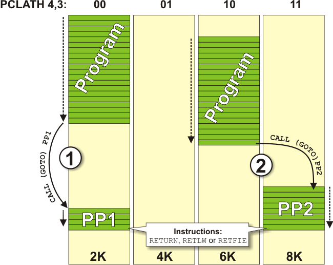
In both cases, when the subroutine reaches instructions
RETURN,
RETLW or
RETFIE (return to the main program), the microcontroller will simply proceed with program execution from where it left off because the return address is pushed and saved onto the stack which, as mentioned, consists of 13-bit registers.
INDIRECT ADDRESSING REGISTERS
In addition to direct addressing, which is logical and clear (it is sufficient to specify the address of a register to read its contents), this microcontroller is capable of performing indirect addressing by means of the INDF and FSR registers. It sometimes makes the process of writing a program easier. The whole procedure is enabled because the INDF register is not true one (physically does not exist), but only specifies the register the address of which is located in the FSR register. For this reason, write or read from the INDF register actually means write or read from the register the address of which is located in the FSR register. In other words, registers’ addresses are specified in the FSR register, and their content is stored in the INDF register. The difference between direct and indirect addressing is illustrated in the figure below:
As seen, the problem with the ‘missing addressing bits’ is solved by a ‘borrow’ from another register. This time, it is the seventh bit, called the IRP bit of the STATUS register.