3.7 CCP Modules
The CCP module (Capture/Compare/PWM) is a peripheral which allows the user to time and control different events.
Capture Mode provides access to the current state of a register which constantly changes its value. In this case, it is the timer TMR1 register.
Compare Mode constantly compares values of two registers. One of them is the timer TMR1 register. This circuit also allows the user to trigger an external event when a predetermined amount of time has expired.
PWM (
Pulse Width Modulation) can generate signals of varying frequency and duty cycle on one or more output pins.
The PIC16F887 microcontroller has two CCP modules- CCP1 and CCP2.
Both of them are identical in normal mode of operation, while the Enhanced PWM features are available on CCP1 only. This is why this chapter gives a detailed description of the CCP1 module. Concerning CCP2, only the features distinguishing it from CCP1 will be covered.
CCP1 MODULE
A central part of this circuit is a 16-bit register CCPR1 which consists of the CCPR1L and CCPR1H registers. It is used for capturing or comparing with binary numbers stored in the timer register TMR1 (TMR1H and TMR1L).
If enabled by software, the timer TMR1 reset may occur on match in Compare mode. Besides, the CCP1 module can generate PWM signals of varying frequency and duty cycle.
Bits of the CCP1CON register are in control of the CCP1 module.
CCP1 IN CAPTURE MODE
In this mode, the timer register TMR1 (consisting of TMR1H and TMR1L) is copied to the CCP1 register (consisting of CCPR1H and CCPR1L) in the following situations:
- Every falling edge (1 -> 0) on the RC2/CCP1 pin;
- Every rising edge (0 -> 1) on the RC2/CCP1 pin;
- Every 4th rising edge (0 -> 1) on the RC2/CCP1 pin; and
- Every 16th rising edge (0 -> 1) on the RC2/CCP1 pin.
A combination of the four bits (CCP1M3 - CCP1M0) of the control register determines which of these events will cause 16-bit data to be transfered. In addition, the following conditions must be met:
- The RC2/CCP1 pin must be configured as an input; and
- TMR1 module must operate as timer or synchronous counter.
The flag bit CCP1IF is set when capture is made. If the CCP1IE bit of the PIE1 register is set when it happens, an interrupt occurs.
When the CCP1 module exsits the capture mode, an unwanted capture interrupt may be generated. In order to avoid this, both a bit enabling CCP1IE interrupt and flag bit CCP1IF should be cleared prior to any change occurs in the control register.
Unwanted interrupts may also be generated by switching from one capture prescaler to another. To avoid this, the CCP1 module should be temporarily switched off before changing the prescaler.
The following program sequence, written in assembly language, is recommended:
BANKESEL CCP1CON
CLRF CCP1CON  ;CONTROL REGISTER IS CLEARED
              ;CCP1 MODULE IS OFF
MOVLW XX      ;NEW PRESCALER MODE IS SELECTED
MOVWF CCP1CON ;NEW VALUE IS LOADED TO THE CONTROL REGISTER
              ;CCP1 MODULE IS SIMULTANEOUSLY SWITCHED ON
Let's do it in mikroC...
...
ASM {
    BANKESEL CCP1CON
    CLRF CCP1CON  // CONTROL REGISTER IS CLEARED
                  // CCP1 MODULE IS OFF
    MOVLW XX      // NEW PRESCALER MODE IS SELECTED
    MOVWF CCP1CON // NEW VALUE IS LOADED TO THE CONTROL REGISTER
}                 // CCP1 MODULE IS SIMULTANEOUSLY SWITCHED ON
...
CCP1 IN COMPARE MODE
In this mode, the value stored in the CCP1 register is constantly compared to the value stored in the timer register TMR1. When a match occurs, the logic state of the RC2/CCP1 output pin may be changed, which depends on the state of bits in the control register (CCP1M3 - CCP1M0). The flag-bit CCP1IF will be simultaneously set.
To set the CCP1 module to operate in this mode, two conditions must be met:
- The RC2/CCP1 pin must be configured as an output; and
- Timer TMR1 must be synchronized with internal clock.
CCP1 IN PWM MODE
Signals of varying frequency and duty cycle have a wide range of application in automation. A typical example is a power control circuit. Refer to figure below. If a logic zero (0) indicates the switch-off and a logic one (1) indicates the switch-on, the electrical power that load consumers will be directly proportional to the pulse duration. This ratio is often called
Duty Cycle.
Another example, common in practice, is the use of PWM signals in the circuit for generating signals of arbitrary waveforms such as sinusoidal waveform. See figure below:
Devices which operate in this way are often used in practice as adjustable frequency drivers controlling the electric motor (speed, acceleration, deceleration etc.).
The figure above shows the block diagram of the CCP1 module set in PWM mode. In order to generate a pulse of arbitrary form on its output pin, it is necessary to set pulse period (frequency) and pulse duration.
PWM PERIOD
The output pulse period (T) is determined by the PR2 register of the timer TMR2. The PWM period can be calculated using the following equation:
PWM Period = (PR2 +1) * 4Tosc * TMR2 Prescale Value
If the PWM period (T) is known, then it is easy to determine the signal frequency F because these two values are related by equation F=1/T.
PWM DUTY CYCLE
The PWM duty cycle is specified by using in total of 10 bits: eight MSbs of the CCPR1L register and two additional LSbs of the CCP1CON register (DC1B1 and DC1B0). The result is a 10-bit number contained in the formula:
Pulse Width = (CCPR1L,DC1B1,DC1B0) * Tosc * TMR2 Prescale Value
The following table shows how to generate PWM signals of varying frequency if the microcontroller uses 20 MHz quartz-crystal (Tosc=50nS).
| FREQUENCY [KHZ] |
1.22 |
4.88 |
19.53 |
78.12 |
156.3 |
208.3 |
| TMR2 Prescaler |
16 |
4 |
1 |
1 |
1 |
1 |
| PR2 Register |
FFh |
FFh |
FFh |
3Fh |
1Fh |
17h |
Just two more things:
- The output pin will be constantly set if the pulse width is by negligence determined to be larger than PWM period.
- In this application, the timer TMR2 postscaler cannot be used for generation of longer PWM periods.
PWM RESOLUTION
An PWM signal is nothing more than a pulse sequence with varying duty cycle. For one specified frequency (number of pulses per second), there is a limited number of duty cycle combinations. This number represents a resolution measured by bits. For example, a 10- bit resolution will result in 1024 discrete duty cycles, whereas an 8-bit resolution will result in 256 discrete duty cycles etc. In relation to this microcontroller, the resolution is determined by the PR2 register. The maximum value is obtained by writing number FFh.
PWM frequencies and resolutions (Fosc = 20MHz):
| PWM FREQUENCY |
1.22KHZ |
4.88KHZ |
19.53KHZ |
78.12KHZ |
156.3KHZ |
208.3KHZ |
| Timer Prescale |
16 |
4 |
1 |
1 |
1 |
1 |
| PR2 Value |
FFh |
FFh |
FFh |
3Fh |
1Fh |
17h |
| Maximum Resolution |
10 |
10 |
10 |
8 |
7 |
6 |
PWM frequencies and resolutions (Fosc = 8MHz):
| PWM FREQUENCY |
1.22KHZ |
4.90KHZ |
19.61KHZ |
76.92KHZ |
153.85KHZ |
200.0KHZ |
| Timer Prescale |
16 |
4 |
1 |
1 |
1 |
1 |
| PR2 Value |
65h |
65h |
65h |
19h |
0Ch |
09h |
| Maximum Resolution |
8 |
8 |
8 |
6 |
5 |
5 |
Let's do it in mikroC...
/* In this example, PWM module is initialized and set to give a pulse train of 50% dutycycle.
For this purpose, functions PWM1_Init(), PWM1_Start() and PWM1_Set_Duty() are used.
All of them are already contained in the mikroC PRO for PIC PWM library and just need to
be copied to the program. */

unsigned short duty_c;     // Define variable duty_c

void initMain() {
    ANSEL = ANSELH = 0;    // All I/O pins are configured as digital
    PORTC = TRISC = 0;     // Initial state of port C output pins
    PWM1_Init(5000);       // PWM module initialization (5KHz)
}

void main() {
    initMain();
    duty_c = 127;          // Initial value of duty-cycle
    PWM1_Start();          // Start PWM1 module
    PWM1_Set_Duty(duty_c); // Set PWM duty-cycle to 50%
    ...
    ...
CCP1CON Register
P1M1, P1M0 - PWM Output Configuration bits - In all modes, except for PWM, the P1A pin is
Capture/Compare module input. P1B, P1C and P1D pins act as input/output port D pins. In PWM mode, these bits affect the operation of the CCP1 module as shown in table below:
| P1M1 |
P1M0 |
MODE |
| 0 |
0 |
PWM with single output |
| Pin P1A outputs modulated signal.
Pins P1B, P1C and P1D are port D input/output |
| 0 |
1 |
Full Bridge - Forward configuration |
| Pin P1D outputs modulated signal
Pin P1A is active
Pins P1B and P1C are inactive |
| 1 |
0 |
Half Bridge configuration |
| Pins P1A and P1B output modulated signal
PinsP1C and P1D are port D input/output |
| 1 |
1 |
Full Bridge - Reverse configuration |
| Pin P1B outputs modulated signal
Pin P1C is active
Pins P1A and P1D are inactive |
DC1B1, DC1B0 - PWM Duty Cycle Least Significant bits - are only used in PWM mode in which they represent two least significant bits of a 10-bit number. This number determines duty cycle of the PWM signal. The rest of bits (8 in total) are stored in the CCPR1L register.
CCP1M3 - CCP1M0 - CCP1 Mode Select bits determine the mode of the CCP1 module.
| CCP1M3 |
CCP1M2 |
CCP1M1 |
CCP1M0 |
MODE |
| 0 |
0 |
0 |
0 |
Module is disabled (reset) |
| 0 |
0 |
0 |
1 |
Unused |
| 0 |
0 |
1 |
0 |
Compare mode |
| CCP1IF bit is set on match |
| 0 |
0 |
1 |
1 |
Unused |
| 0 |
1 |
0 |
0 |
Capture mode |
| Every falling edge on the CCP1 pin |
| 0 |
1 |
0 |
1 |
Capture mode |
| Every rising edge on the CCP1 pin |
| 0 |
1 |
1 |
0 |
Capture mode |
| Every 4th rising edge on the CCP1 pin |
| 0 |
1 |
1 |
1 |
Capture mode |
| Every 16th rising edge on the CCP1 pin |
| 1 |
0 |
0 |
0 |
Compare mode |
| Output and CCP1IF bit are set on match |
| 1 |
0 |
0 |
1 |
Compare mode |
| Output is cleared and CCP1IF bit is set on match |
| 1 |
0 |
1 |
0 |
Compare mode |
| Interrupt request arrives and bit CCP1IF is set on match |
| 1 |
0 |
1 |
1 |
Compare mode |
| Bit CCP1IF is set and timers 1 or 2 registers are cleared |
| 1 |
1 |
0 |
0 |
PWM mode |
| Pins P1A and P1C are active-high
Pins P1B and P1D are active-high |
| 1 |
1 |
0 |
1 |
PWM mode |
| Pins P1A and P1C are active-high
Pins P1B and P1D are active-low |
| 1 |
1 |
1 |
0 |
PWM mode |
| Pins P1A and P1C are active-low
Pins P1B and P1D are active-high |
| 1 |
1 |
1 |
1 |
PWM mode |
| Pins P1A and P1C are active-low
Pins P1B and P1D are active-low |
CCP2 MODULE
Excluding the different names of registers and bits, this module is a very good copy of the CCP1 module set in normal mode. There is only one true difference between them when CCP2 operates in Compare mode.
The difference refers to the timer T1 reset signal. Namely, if A/D converter is enabled, at the moment the values of the TMR1 and CCPR2 registers match, the timer T1 reset signal will automatically start A/D conversion.
Similar to the pervious module, this circuit is also under control of the control register bits. This time, it is the CCP2CON register.
CCP2CON Register
DC2B1, DC2B0 - PWM Duty Cycle Least Significant bits - are only used in PWM mode representing two least significant bits of a 10-bit number. This number determines duty cycle of the PWM signal. The rest of bits (8 in total) are stored in the CCPR2L register.
CCP2M3 - CCP2M0 - CCP2 Mode Select bits select CCP2 mode.
| CCP2M3 |
CCP2M2 |
CCP2M1 |
CCP2M0 |
MODE |
| 0 |
0 |
0 |
0 |
Module is disabled (reset) |
| 0 |
0 |
0 |
1 |
Unused |
| 0 |
0 |
1 |
0 |
Unused |
| 0 |
0 |
1 |
1 |
Unused |
| 0 |
1 |
0 |
0 |
Capture mode |
| Every falling edge on the CCP2 pin |
| 0 |
1 |
0 |
1 |
Capture mode |
| Every raising edge on the CCP2 pin |
| 0 |
1 |
1 |
0 |
Capture mode |
| Every 4th rising edge on the CCP2 pin |
| 0 |
1 |
1 |
1 |
Capture mode |
| Every 16th rising edge on the CCP2 pin |
| 1 |
0 |
0 |
0 |
Compare mode |
| Output and CCP2IF bit are set on match |
| 1 |
0 |
0 |
1 |
Compare mode |
| Output is cleared and CCP2IF bit is set on match |
| 1 |
0 |
1 |
0 |
Compare mode |
| Interrupt is generated, CCP2IF bit is set and CCP2 pin is unaffected on match |
| 1 |
0 |
1 |
1 |
Compare mode |
| CCP2IF bit is set, Timer 1 registers are cleared, A/D conversion is started if the A/D converter is on on match |
| 1 |
1 |
x |
x |
PWM mode |
In Short
Setting up CCP1 module for PWM operation
In order to set up the CCP module for PWM operation, the following steps should be taken:
- Disable the CCP1 output pin. It should be configured as an input.
- Set the PWM period by loading the PR2 register.
- Configure the CCP module to operate in the PWM mode by combining bits of the CCP1CON register.
- Set duty cycle of the PWM signal by loading the CCPR1L register and using bits DC1B1 and DC1B0 of the CCP1CON register.
- Configure and start timer TMR2:
- Clear the TMR2IF interrupt flag bit of the PIR1 register.
- Set the timer TMR2 prescale value by loading bits T2CKPS1 and T2CKPS0 of the T2CON register.
- Start the timer TMR2 by setting the TMR2ON bit of the T2CON register.
- Enable PWM output pins after one PWM cycle has been complete:
- Wait for the timer TMR2 overflow (the TMR2IF bit of the PIR1register is set).
- Configure the appropriate pin as an output by clearing the bit of the TRIS register.
CCP1 IN ENHANCED MODE
The enhanced mode is available on CCP1 only. The CCP1 in enhanced mode basically doesn’t differ from the CCP1 in normal mode and enhancement refers to transmission of PWM signal to the output pins. Why is it so important? Because the microcontrollers are more frequently used in electric motor control systems. These devices are not described herein, but if you ever have had a chance to work on development of similar devices, you will recognize elements which, until quite recently, were used as external ones. We say ‘were used’ because all these elements are now integrated into the microcontroller and can operate in several different modes.
SINGLE OUTPUT PWM MODE
A single output PWM mode is enabled only in the event that the P1M1 and P1M0 bits of the CCP1CON register are cleared. In this case, one PWM signal can be simultaneously available on maximum of four different output pins. Besides, the PWM signal may appear in basic or inverted waveform. Signal distribution depends on the bits of the PSTRCON register, while its polarity depends on the CCP1M1 and CCP1M0 bits of the CCP1CON register.
When an inverted output is in use, pins are low-active and pulses having the same waveform are always generated in pairs: on the P1A and P1C pins and P1B and P1D pins, respectively.
HALF-BRIDGE MODE
In relation to the half-bridge mode, the PWM signal is the output on the P1A pin, while at the same time the complementary PWM signal is the output on the P1B pin. Such pulses activate MOSFET drivers in
Half-Bridge mode which enable/disable current flow through the device.
It is very dangerous to switch on MOSFET drivers simultaneously. The short circuit caused in that moment will be fatal. In order to avoid this, it is necessary to provide a short delay between switching drivers on and off. Such delay is marked as 'td' in figure below. The problem is solved by using the PDC0-PDC6 bits of the PWM1CON register.
As shown in figure below, the half-bridge mode can also be used to activate MOSFET drivers in the
Full Bridge configuration:
FULL-BRIDGE MODE
All four pins are used as outputs in the full-bridge mode. In practice, this mode is commonly used to run motors, thus providing a simple and full control of speed and rotation direction. There are two configurations of this mode:
Full Bridge-Forward and
Full Bridge-Reverse.
FULL BRIDGE - FORWARD CONFIGURATION
In
Forward mode the following occurs:
- Logic one (1) appears on the P1A pin (pin is active-high);
- Pulse sequence appears on the P1D pin; and
- Logic zero (0) appears on the P1B and P1C pins (pins are active-low).
Figure below shows the state of the P1A-P1D pins during one full PWM cycle.
FULL BRIDGE - REVERSE CONFIGURATION
The similar occurs in
Reverse mode, only that these pins have different functions:
- Logic one (1) appears on the P1C pin (pin is active-high);
- Pulse sequence appears on the P1B pin; and
- Logic zero (0) appears on the P1A and P1D pins (pins are active-low).
PWM1CON Register
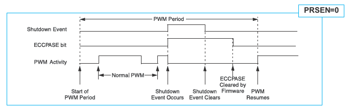
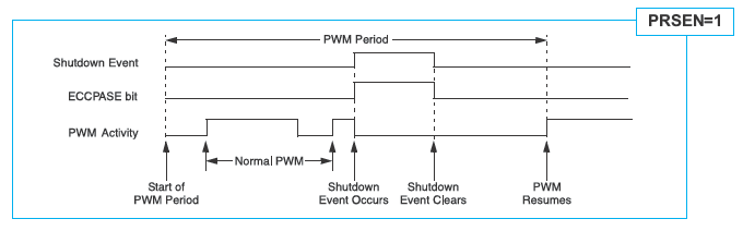
STRC PWM Restart Enable bit
- 1 - Upon auto-shutdown, the PWM module automatically restarts, while the ECCPASE bit of the ECCPAS register is cleared.
- 0 - In order to restart PWM module upon auto-shutdown, the ECCPASE bit must be cleared in software.
PDC6 - PDC0 PWM Delay Count bits - 7-digit binary number determines the number of instruction cycles (4*Tosc) added as a time delay during activation of PWM output pins.
PSTRCON Register
STRSYNC - Steering Sync bit determines the moment of PWM pulse steering:
- 1 - Steering occurs upon the PSTRCON register has been changed, but only if a PWM waveform is completed.
- 0 - Steering occurs upon the PSTRCON register has been changed. The PWM signal on the output pin is immediately changed with no regard to whether the previous cycle is completed or not. This operation is useful when it is needed to immediately remove a PWM signal from the pin.
STRD - Steering Enable bit D determines the P1D pin function.
- 1 - The P1D pin has the PWM waveform with polarity controlled by the CCP1M0 and CCP1M1 bits.
- 0 - Pin is configured as a general port D input/output.
STRC Steering Enable bit C determines the P1C pin function.
- 1 - The P1C pin has the PWM waveform with polarity controlled by the CCP1M0 and CCP1M1 bits.
- 0 - Pin is configured as a general port D input/output.
STRB - Steering Enable bit B determines the P1B pin function.
- 1 - The P1B pin has the PWM waveform with polarity controlled by the CCP1M0 and CCP1M1 bits.
- 0 - Pin is configured as a general port D input/output.
STRA - Steering Enable bit A determines the P1A pin function.
- 1 - The P1D pin has the PWM waveform with polarity controlled by the CCP1M0 and CCP1M1 bits.
- 0 - Pin is configured as a general port C input/output.
ECCPAS Register
ECCPASE - ECCP Auto-Shutdown Event Status bit indicates whether shut-down of CCP module has occurred (
Shutdown state):
- 1 - CCP module is in Shutdown state.
- 0 - CCP module operates normally.
ECCPAS2 - ECCPAS0 - ECCP Auto-Shutdown Source Select bits select auto shutdown source:
| ECCPAS2 |
ECCPAS1 |
ECCPAS0 |
SHUTHOWN STATE SOURCE |
| 0 |
0 |
0 |
Shutdown state disabled |
| 0 |
0 |
1 |
Comparator C1 output change |
| 0 |
1 |
0 |
Comparator C2 output change |
| 0 |
1 |
1 |
Comparator C1 or C2 output change |
| 1 |
0 |
0 |
Logic zero (0) on INT pin |
| 1 |
0 |
1 |
Logic zero (0) on INT pin or comparator C1 output change |
| 1 |
1 |
0 |
Logic zero (0) on INT pin or comparator C2 output change |
| 1 |
1 |
1 |
Logic zero (0) on INT pin or comparator C1 or C2 output change |
PSSAC1, PSSAC0 - Pins P1A, P1C Shutdown State Control bits define the logic state of output pins P1A and P1C when CCP module is in shutdown state.
| PSSAC1 |
PSSAC0 |
PINS LOGIC STATE |
| 0 |
0 |
0 |
| 0 |
1 |
1 |
| 1 |
X |
High impedance (Tri-state) |
PSSBD1, PSSBD0 - Pins P1B, P1D Shutdown State Control bits define the logic state of output pins P1B and P1D when CCP module is in shutdown state.
| PSSBD1 |
PSSBD0 |
PINS LOGIC STATE |
| 0 |
0 |
0 |
| 0 |
1 |
1 |
| 1 |
X |
High impedance (Tri-state) |
The PIC16F887 microcontroller has several independent serial communication modules, and each of them can be configured to operate in several different modes, which make them irreplaceable in many situations. Remember what we advised you about the CCP modules as the same applies here. Don’t burden yourself with details of the operation of all of them, but select one and use only what you really need.