1.3 Must Know Details
The operation of logic circuits is based on principles established by a British mathematician George Boole in the middle of the 19th century, even before the first bulb was invented. Originally, the main idea was to express logical forms through algebraic functions. It soon had lead to a real product which, much later, evaluated in what today is known as AND, OR and NOT logic circuits. The principle of their operation is known as Boolean algebra.
LOGIC CIRCUITS
Some of the program instructions give the same results as logic gates. The principle of their operation will be discussed below.
AND Gate
The logic gate ‘AND’ has two or more inputs and one output. Let us presume that the gate used in this example has only two inputs. A logic one (1) will appear on its output only if both inputs (A AND B) are driven high (1). Table on the right shows mutual dependence between the AND gate’s inputs and output.
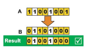
The principle of operation is the same even when the gate has more than two inputs: a logic one (1) will appear on its output only when all inputs are driven high (1). Any other combination of input voltages will result in a logic zero (0) on its output. When used in the program, the logic AND is performed by a program instruction to be discussed later. Just remember that logic AND in the program refers to the corresponding bits of tworegisters.
OR GATE
Similarly, OR gates also have two or more inputs and one output. If the gate has only two inputs the following applies. A logic one (1) will appear on its output if either input (A OR B) is driven high (1). If the OR gate has more than two inputs then the following applies. A logic one (1) appears on its output if at least one input is driven high (1). If all inputs are at logic zero (0), the output will be at logic zero (0) as well.
In the program, the peration is performed in the same manner as the logic AND operation.
NOT GATE
The logic gate NOT has only one input and only one output. It operates in an extremely simple way. When a logic zero (0) appears on its input, a logic one (1) appears on its output and vice versa. It means that this gate inverts the signal and is therefore often called inverter.

The logic NOT operation in the program is performed upon one byte. The result is a byte with inverted bits. If byte bits are considered a number, the inverted value is actually a complement thereof. The complement of a number is a value which added to that number makes it reach the largest 8-digit binary number. In other words, the sum of an 8-digit number and its complement is always 255.
EXCLUSIVE OR GATE
The EXCLUSIVE OR (XOR) gate is a bit complicated compared to other gates. It is a sort of combination of all of them. A logic one (1) appears on its output only when its inputs have different logic states.
In the program, the appropriate instruction is commonly used to compare two bytes. Subtraction has the same purpose (if the result is 0, bytes are equal), but the advantage of the EXCLUSIVE OR logic operation is that it never gives negative results.
REGISTER
In short, a register or a memory cell is an electronic circuit which can memorize the state of one byte.
SFR REGISTERS
In addition to registers which do not have any special and predefined function, every microcontroller also has a number of special-function registers (SFR’s) the function of which is predefined by the manufacturer. Their bits are connected (literally) to the integrated circuits within the microcontroller such as timers, A/D converter, oscillators etc. It means that they are directly in command of the operation of these circuits, i.e. the microcontroller. Imagine eight switches controlling the operation of a small circuit within the microcontroller - Special Function Registers do exactly that.

In other words, the state of register bits is changed from within the program, registers run small integrated circuits within the microcontroller, these circuits are via microcontroller pins connected to peripherals which are used for... Well, it’s up to you to decide for what.
INPUT / OUTPUT PORTS
In order for the microcontroller to be useful, it has to be connected to additional electronics, i.e. peripherals. Each microcontroller has one or more registers connected to the microcontroller I/O pins. Such connections make I/O ports. Why input/output? Because you can change a pin function as you wish. For example, suppose you want your device to turn on/off three signal LEDs and simultaneously monitor the logic state of five sensors or push buttons. Some of the ports need to be configured so as to have three outputs (connected to LEDs) and five inputs (connected to sensors). It can be easily done from within the software, which means that a pin function can be changed during the operation.
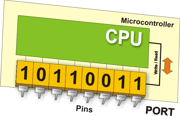
One of the important features of input/output (I/O) pins is a maximum current they can handle. For most microcontrollers, current supplied from one pin is sufficient to activate a LED or some other low-consumption device (10-20 mA).
Another important pin feature is a pull-up resistor it may be provided with. The pull-up resistor connects the appropriate pin to the positive power supply voltage. It can also be used when the pin is configured as an input connected to a switch or a push button. Later versions of microcontrollers have pull-up resistors configurable by software.
Each I/O port is usually under control of one SFR, which means that each bit of that register determines the state of the corresponding microcontroller pin. For example, by writing a logic one (1) to some of the register bits, the appropriate microcontroller pin is automatically configured as an input. The voltage supplied to that pin is visible on its port as 0 or 1. Otherwise, by writing a logic zero to the SFR, the appropriate port pin is configured as an output. Voltage provided on such an output pin (0V or 5V) reflects the state of the appropriate register bit (logic 0 or 1, respectively).
MEMORY UNIT
Memory module is a part of the microcontroller used for data storage. The easiest way to explain it is by comparing it with a filing cabinet with many drawers. Suppose, the drawers are clearly marked so that their contents can be easily available by reading labels on the front of the drawers. In the same way, each memory address corresponds to one memory location. The contents of any location can be accessed and read by its address. Memory can either be written to or read from.
There are several types of memory within the microcontroller:
READ ONLY MEMORY (ROM)
Read Only Memory (ROM) is used to permanently save the program to be executed by the microcontroller. The size of a program to be written depends on the size of this memory. Today’s microcontrollers commonly use 16-bit addressing, which means that they are able to address up to 64 Kb of memory, i.e. 65535 locations. If you are a novice, your program will hardly exceed several hundred instructions. There are several types of ROM.
Masked ROM (MROM)
Masked ROM is a special type of ROM the content of which is determined by the manufacturer. The term ‘masked’ comes from the manufacturing process, where parts of the chip are masked off before the process of photolithography. In case of a large-scale production, the price is very low. Forget it...
One Time Programmable ROM (OTP ROM)
One time programmable ROM enables you to download a program into it, but, as its name states, one time only. If an error is detected after the process of loading a program, the only thing you can do is to load the program to another chip.
UV ERASABLE PROGRAMMABLE ROM (UV EPROM)
Both the manufacturing process and characteristics of UV EPROM memory are fully identical to OTP ROM. However, the package of the microcontroller with this memory has a recognizable ‘window’ on its top side. It enables data to be erased under strong ultraviolet light. After a few minutes of such ‘sunbathing’ it is possible to load a new program into it. The installation of this window is complicated, which normally affects the price. In our opinion, unfortunately negative...
Flash Memory
Flash memory, known as the successor to the UV EPROM, was made in the 80s in the laboratories of INTEL. Since such memory can be rewritten practically an unlimited number of times, microcontrollers with Flash ROM are ideal for learning, experimentation and small-scale production. Due to its great popularity, most microcontrollers are today manufactured in flash technology. So, if you are going to buy a microcontroller, the type to look for is definitely Flash!
RANDOM ACCESS MEMORY (RAM)
Once the power supply is off the contents of RAM is cleared. It is therefore used for temporary storing data and intermediate results created and used during the operation of the microcontroller. For example, if the program performs an addition, it is necessary to have a register which stands for what in everyday life is called the ‘sum’. For this reason, one of the registers of RAM is called the ‘sum’ and used for storing results of addition.
ELECTRICALLY ERASABLE PROGRAMMABLE ROM (EEPROM)
The contents of EEPROM may be changed during operation (similar to RAM), but remains permanently saved even after the loss of power (similar to ROM). Accordingly, EEPROM is often used to store values, created during operation, which must be permanently saved. For example, if you design an electronic lock or an alarm, it would be great to enable the user to create and enter the password, but it’s useless if lost every time the power supply goes off. The ideal solution is a microcontroller with an embedded EEPROM.
INTERRUPT
Most programs use interrupts in their regular execution. The purpose of the microcontroller is mainly to respond to changes in its surrounding. In other words, when an action takes place, the microcontroller does something... For example, when you push a button on a television remote control, the microcontroller will register it and respond by changing a channel, turn the volume up or down etc. As such, the microcontroller would spend most of its time endlessly checking a few buttons for hours or days, which is not practical at all.
This is why the microcontroller has learnt a trick during its evolution. Instead of constant checking each pin or bit, the microcontroller delegates the ‘wait issue’ to a ‘specialist’ which will respond only when something attention worthy happens.
A signal which informs the central processor unit about such action is called an INTERRUPT.
BUS
A bus consists of 8, 16 or more wires. There are two types of buses: the address bus and the data bus. The address bus consists of as many lines as necessary for memory addressing. It is used to tranfer an address from the CPU to the memory. The data bus is as wide as data, in this case it is 8 bits or wires wide. It is used to connect all the circuits within the microcontroller.
CENTRAL PROCESSOR UNIT (CPU)
As its name suggests, the CPU is a unit which monitors and controls all processes within the microcontroller. It consists of several subunits, of which the most important are:
- Instruction Decoder decodes program instructions and runs other circuits on the basis of that;
- Arithmetical Logical Unit (ALU) performs all mathematical and logical operations upon data. The ‘instruction set’ which is different for each microcontroller family shows the abilities of this circuit; and
- Accumulator is an SFR closely related to the operation of the ALU. It is a kind of working desk used for storing all data upon which some operation is to be performed (addition, shift/move etc.). It also stores results to be used in further processing. One of the SFRs, called a Status Register (PSW), is closely related to the accumulator. It shows, at any given time, the ‘status’ of a number stored in the accumulator (number is larger or less than zero etc.). The accumulator is also called the working register and is referred to as W register or just W therefore.
SERIAL COMMUNICATION
A parallel connection between the microcontroller and peripherals established via input/output ports is an ideal solution when the distance between them is up to several meters. Otherwise, when it is necessary to establish communication on longer distances the parallel connection is out of the question. Serial communication is used instead.
Today, most microcontrollers have several different modules for serial communication built into them as a standard equipment. Which of these modules will be used depends on many factors of which the most important are:
- How many devices the microcontroller has to exchange data with?
- How fast does the data exchange have to be?
- What is the distance between devices?
- Is it necessary to send and receive data simultaneously?
One of the most important things about the serial communication is the
Protocol which should be strictly observed. It is a set of rules which enables devices to correctly interpret data they exchange. Fortunately, the microcontroller itself takes care of this, so that the work of the programmer/user boils down to simple writing (data to be sent) and reading (received data).
DATA RATE
The term
data rate is used to denote the number of bits transferred per second [bps]. Note that it refers to bits, not bytes. According to the protocol, each byte is transferred along with several control bits. It means that one byte in serial data stream may consist of 11 bits. For example, if the data rate is 300 bps then maximum 37 and minimum 27 bytes may be transferred per second.
The most commonly used serial communication modules are:
I2C (INTER INTEGRATED CIRCUIT)
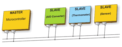
An inter-integrated circuit is a module for serial data exchange between microcontrollers and specialized integrated circuits of a new generation. It is used when the distance between these devices is short (receiver and transmitter are usually on the same printed board). The connection is established via two conductors. One is used for data transfer, while the other is used for synchronization (clock signal). As can be seen in figure below, one device is always a master device. It performs addressing of one slave device before communication starts and controls the process of data transfer. In this way one microcontroller can communicate with 112 different devices using I2C. Data rate is usually 100 Kb/sec (standard mode) or 10 Kb/sec (slow data rate mode). Devices with a data rate of 3.4 Mb/sec have recently appeared. The distance between devices which communicate over an I2C bus is limited to several meters.
SPI (SERIAL PERIPHERAL INTERFACE BUS)
A serial peripheral interface (SPI) bus is a module for serial communication which uses three or four conductors. One conductor is used to receive data, one to send data, one for synchronization and one alternatively for selecting a device to communicate with. It is a
full duplexconnection, which means that data can be sent and received simultaneously.
The maximum data rate is higher than that in the I2C communication module.
UART (UNIVERSAL ASYNCHRONOUS RECEIVER/TRANSMITTER)
As its name suggests, the USART communication is asynchronous, which means that no special line for clock signal transfer is used. In some applications, such as radio connection or infrared waves remote control, this feature is crucial. Since only one communication line is used, both receiver and transmitter operate at the same predefined rate in order to maintain necessary synchronization. This is a very simple way of transferring data as it basically comes down to the conversion of 8-bit data from parallel to serial format. Data rate is not high, up to 1 Mbit/sec.
OSCILLATOR
Even pulses generated by the oscillator enable a harmonic and synchronous operation of all circuits within the microcontroller. The oscillator is usually configured so as to use a quartz crystal or ceramic resonator for frequency stabilization, but it can also operate as a stand-alone circuit (like RC oscillator). It is important to say that instructions are not executed at the rate imposed by the oscillator itself, but several times slower. It happens because each instruction is executed in several steps. In some microcontrollers, the same number of cycles is required to execute all instructions, while in others, the number of cycles is different for different instructions. Accordingly, if the microcontroller uses quartz crystal with a frequency of 20 Mhz, the execution time of an instruction is not 50nS, but 200, 400 or 800 nS, depending on the microcontroller type.
POWER SUPPLY CIRCUIT
There are two things worth attention when speaking of the microcontroller power supply circuit:
- Brown out is a potentially dangerous condition which occurs at the moment the microcontroller is turned off or when the power supply voltage drops to its minimum value due to noise. As the microcontroller consists of several circuits with different operating voltage levels, such condition can cause its out-of-control performance. In order to prevent it, the microcontroller usually has a built-in reset circuit which causes the reset condition to occur as soon as the microcontroller goes into a brown out state of emergency.
- Reset pin is usually referred to as MCLR (Master Clear Reset). It is used for causing an external reset of the microcontroller by applying a logic zero (0) or a logic one (1) to it, which depends on the type of the microcontroller. In case the brown out circuit is not built into the microcontroller, a simple external circuit for brown out reset can be connected to the MCLR pin.
TIMERS/COUNTERS
The microcontroller oscillator uses quartz crystal for its operation. Even though it is not the best solution, there are still many reasons to use it. The frequency of such oscillator is precisely defined and very stable, so that pulses it generates are always the same width, which makes them ideal for time measurement. Such oscillators are also used in quartz watches. If it is necessary to measure time between two events, it is sufficient to count up pulses generated by this oscillator. This is exactly what the timer does.
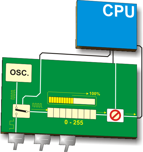
Most programs use these miniature electronic ‘stopwatches’. Their heart make 8- or 16- bit SFRs, the contents of which is automatically incremented by each coming pulse. Once a register is fully loaded, an interrupt may be generated.
If the timer uses an internal quartz oscillator for its operation, then it can be used to measure time between two events (if the value stored in the timer register is T1 at the moment the measurement starts, and T2 at the moment it terminates, then the time elapsed is equal to the result of subtraction T2-T1). If registers use pulses supplied from an external source then such timer is turned into a counter.
This is just a simple explanation of the operation of timer/counter. As you already know, it is more complicated in practice.
HOW DOES THE TIMER OPERATE?
This is how the timer operates in practice: pulses generated by the quartz oscillator are directly, or via a prescaler, brought to the circuit which increments the number stored in the timer register. By embedding a quartz crystal with a frequency of 4MHz the following applies: if one instruction (one machine cycle) lasts for four quartz oscillator periods then by embedding a quartz crystal with a frequency of 4MHz this number will be incremented a million times per second (each microsecond).
It is easy to measure short time intervals, up to 256 microseconds, in the way described above because it is the largest number that one register can store. This restriction may be easily made up by using a slower oscillator, registers with more bits, prescaler or interrupts. The first two solutions have some drawbacks so that it is more advisable to use prescalers or interrupts.
USING A PRESCALER IN TIMER OPERATION
A prescaler is an electronic device used to reduce frequency by a predefined division rate. In order to generate one pulse on its output, it is necessary to bring 1, 2, 4 or more pulses on its input. Most microcontrollers have one or more bulit-in prescalers and their division rate may be changed from within the program. The prescaler is used when it is necessary to measure longer periods of time.
USING INTERRUPT IN TIMER OPERATION
If the timer register consists of 8 bits, the largest number it can store is 255. For 16-bit registers it is the number 65.535. If such number is exceeded, the timer will be automatically reset and counting will start from zero again. This condition is called an
overflow. If enabled from within the program, the overflow can cause an interrupt, which gives completely new possibilities. For example, the state of registers used for counting seconds, minutes or days can be changed in an interrupt routine. The whole process (except for the interrupt routine) is automatically performed behind the scenes, which enables the main circuits of the microcontroller to operate normally.
Figure above illustrates the use of an interrupt in timer operation. Delays of arbitrary duration, having almost no influence on the main program execution, can be easily obtained by assigning a prescaler to the timer.
COUNTERS
If the timer is supplied with pulses from the microcontroller input pin, then it turns into a counter. It is clear that the same electronic circuit is able to operate in two different modes. The only difference is that in this case pulses to be counted come via the microcontroller input pin and their duration (width) is usually undefined. This is why they cannot be used for time measurement, but can be used for other purposes such as counting products on an assembly line, number of axis rotation, passengers etc. (depending on sensor in use).
WATCHDOG TIMER
A watchdog timer is a timer connected to a stand-alone RC oscillator within the microcontroller.
If the watchdog timer is enabled, every time it counts up to the maximum value, the microcontroller reset occurs and the program execution starts from the first instruction. The point is to prevent this from happening by using a specific command.
Anyway, the whole idea is based on the fact that every program is executed in several longer or shorter loops. If instructions for the watchdog timer reset are set at the appropriate program locations, in addition to commands being regularly executed, then the operation of the watchdog timer will not affect the program execution. If for any reason, usually due to manufacturing noise, the program counter ‘gets stuck’ at some memory location from which there is no return, the watchdog timer will not be cleared, so the register’s value being constantly incremented will reach the maximum
et voila! Reset occurs and the program will be executed from the beginning.
A/D CONVERTER
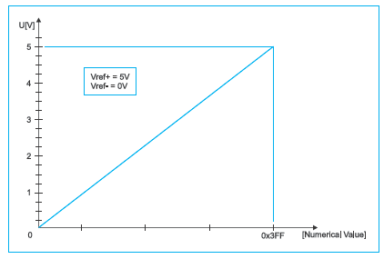
External signals are usually fundamentally different from those the microcontroller recognizes (0V and 5V only) and therefore have to be converted into recognizable values. An analog to digital converter is an electronic circuit which converts continuous signals to discrete digital numbers. In other words, this circuit converts an analogue value into a binary number and forwards it to the CPU for further processing. This module is thus used for input pin voltage (analogue value) measurement.
The result of measurement is a number (digital value) used and processed later in the program.
INTERNAL ARCHITECTURE
All upgraded microcontrollers implement one of the two basic design models called
Harvard and
von-Neumann architecture.
They represent two different ways of exchanging data between the CPU and memory.
VON-NEUMANN ARCHITECTURE
Microcontrollers using the von-Neumann architecture have only one memory block and one 8-bit data bus. As all data is exchanged through these 8 lines, the bus is overloaded and communication is slow and inefficient. The CPU can either read an instruction or read/write data from/to the memory. Both processes cannot be performed at the same time since instructions and data use the same bus. For example, if a program line reads that a RAM memory register called ‘SUM’ should be incremented by one (instruction: incf SUM), the microcontroller will do the following:
- Read the part of the program instruction specifying WHAT should be done (in this case the ‘
incf’ instruction for increment is to be performed).
- Read the other part of the same instruction specifying upon WHICH data it should be performed (in this case it is the ‘SUM’ register).
- After being incremented, the contents of this register should be written to the register from which it was read (the address of the ‘SUM’ register).
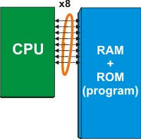
The same data bus is used for all these intermediate operations when data is exchanged between the CPU and memory.
HARVARD ARCHITECTURE
Microcontrollers which implement the Harvard architecture have two different data buses. One is 8 bits wide and connects the CPU to RAM. The other consists of 12, 14 or 16 lines and connects the CPU to ROM. Accordingly, the CPU can read an instruction and access data memory at the same time. Since all RAM memory registers are 8 bits wide, all data being exchanged is of the same width. During the writing process, only 8-bit data is included. In other words, all you can change from within the program and all you can deal with is 8 bits wide. All the programs written for these microcontrollers will be stored in the microcontroller internal ROM after being compiled to machine code. However, ROM memory locations are not 8, but 12, 14 or 16 bits wide. The rest of bits 4, 6 or 8, respectively, represents the instruction alone specifying for the CPU what to do with the 8-bit data.
The advantages of this architecture are as follows:
- All data in the program is one byte (8 bits) wide. As the data bus used for program reading has 12, 14 or 16 lines, both instruction and data can be read simultaneously using these spare bits. For this reason, all instructions are single-cycle instructions, except the jump instruction which is two-cycle.
- Owing to the fact that the program (ROM) and temporary data (RAM) use separate buses, the CPU can execute two instructions at the same time. In other words, while RAM read or write is in progress (the end of one instruction), the next program instruction is read via the other bus.
- With microcontrollers with the von-Neumann architecture, one never knows how much memory is to be occupied by the program. Basically, most program instructions occupy two memory locations (one contains information on WHAT should be done, while the other contains information upon WHICH data it should be done). However, it is not a hard and fast rule, but the most common case. In the Harvard architecture the program bus is wider than one byte, which allows each program word to consist of instruction and data, i.e. one memory location - one program instruction.
INSTRUCTION SET
All instructions recognizable by the microcontroller are colectivelly called the Instruction Set. When you write a program in assembly language, you actually specify instructions in such order as they should be executed. The main restriction here is the number of available instructions. The manufacturers usually employ one of the two opposite solutions and design microcontrollers which implement the smallest or the largest possible number of instructions. In other words - they choose between RISC and CISC instruction sets, respectively.
RISC (REDUCED INSTRUCTION SET COMPUTER)
In this case, the microcontroller recognizes and executes basic operations only (addition, subtraction, copying etc.). Other, more complicated operations are performed by combining them. For example, multiplication in the program must be performed as a successive addition. It’s the same as if you try to explain to someone, using only a few different words, how to reach the airport in a big city. However, it’s not as black as it’s painted. As a matter of fact, it is not so difficult to explain where the airport is if you use the right words such as left, right, kilometers etc.
CISC (COMPLEX INSTRUCTION SET COMPUTER)
CISC is the opposite to RISC. Microcontrollers designed to recognize more than 200 different instructions can do a lot of things at high speed. However, one needs to understand how to take all that such a rich instruction set offers, which is not easy at all...
HOW TO MAKE THE RIGHT CHOICE?
OK, you are a beginner and you have made a decision to go on an adventure of working with microcontrollers. Congratulations on your choice. But, it is not as easy to choose the right microcontroller as it may seem. The problem is not a limited range of devices, but the opposite.
Before you start designing a microcontroller-based device, think of the following: how many inputs/outputs does your project require? Should it perform some other operations than to simply turn relays on/off? Does it need some specialized modules such as serial communication, A/D converter etc.? When you create a clear picture of what you need, the selection range is considerably reduced and it’s time to think of the price. Are you going to make several such devices? Several hundred? A million? Anyway, you get the point.
If you think of all these things for the very first time then everything seems a bit complicated. Make it simple and go step by step. First of all, select the manufacturer, i.e. the microcontroller family you can easily get. Study one particular model. Learn as much as you need, don’t go into details. Solve a specific problem and something incredible will happen- you will be able to handle any model belonging to that microcontroller family.
Remember learning to ride a bicycle. After several bruises you got when you started, you were able to keep the balance and then easily ride any other bicycle. And of course, you will never forget programming just as you will never forget riding bicycles!


 The logic NOT operation in the program is performed upon one byte. The result is a byte with inverted bits. If byte bits are considered a number, the inverted value is actually a complement thereof. The complement of a number is a value which added to that number makes it reach the largest 8-digit binary number. In other words, the sum of an 8-digit number and its complement is always 255.





 The same data bus is used for all these intermediate operations when data is exchanged between the CPU and memory.

