3.3 Input/Output Ports
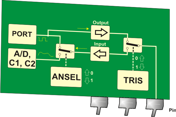
One of the most important merits of the microcontroller is a number of input/output pins which enable it to be connected to peripheral modules. There are in total 35 general-purpose I/O pins provided on the PIC16F887, which is quite enough for most applications.
In order to synchronize the operation of I/O ports with the internal 8-bit organization of the microcontroller, they are, similar to registers, grouped into five ports denoted by letters A, B, C, D and E. All I/O ports have several features in common:
- To save more space on the board, all I/O pins are multifunctional. However, they can be assigned only one function at the same time.
- Every port is accompanied by the corresponding TRIS register: TRISA, TRISB, TRISC etc. which determines the performance, but not the contents of the port bits. By clearing any bit of the TRIS register (bit=0), the corresponding port pin is configured as an output. Similarly, by setting any bit of the TRIS register (bit=1), the corresponding port pin is configured as an input. This rule is easy to remember 0 = Output, 1 = Input.
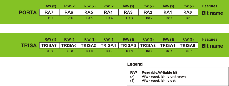
PORTA and TRISA register
Port PORTA is an 8-bit wide, bidirectional port. Bits of the TRISA register control the PORTA pins, i.e. whether they will act as digital inputs or outputs:

Similar to the TRISA register bits which determine which of the pins are to be configured as inputs and which ones as outputs, the appropriate bits of the ANSEL register determine whether PORTA pins are to be configured as analog inputs or digital inputs/outputs.
RA0 = AN0 (determined by the ANS0 bit of the ANSEL register)
RA1 = AN1 (determined by the ANS1 bit of the ANSEL register)
RA2 = AN2 (determined by the ANS2 bit of the ANSEL register)
RA3 = AN3 (determined by the ANS3 bit of the ANSEL register)
RA5 = AN4 (determined by the ANS4 bit of the ANSEL register)
Each bit of this port is assigned an additional function related to some of the built-in peripheral modules. This chapter covers only the RA0 pin’s additional function which is related to the PORTA and ULPWU unit, whereas additional function of other pins will be described in later chapters.
Let's do it in mikroBasic...
' The PORTA.2 pin is configured as a digital input. All other PORTA pins are digital ... outputs
ANSEL = ANSELH = 0 ' All I/O pins are configured as digital
PORTA = 0 ' All PORTA pins are cleared
TRISA = %00000100 ' All PORTA pins except PORTA.2 are configured as outputs
...
ULPWU UNIT
The microcontroller is commonly used in independent battery powered devices which operate periodically. Typical examples are thermometers, fire detection sensors and the like. Minimum power consumption is one of the priorities here. As a reduction in clock frequency causes the power consumption to be reduced, one of the most convenient solutions to this issue is to slow down the clock, that is to say to use 32KHz quartz crystal instead of 20MHz.
Setting the microcontroller to sleep mode is a step further in the same direction. Here we come to another issue - how to wake up the microcontroller and set it to normal mode? Obviously, it is necessary to somehow provide an external signal to change the logic state of some pin. The only way to do it is by means of additional electronics, which on the other hand causes higher power consumption of the entire device...
The ideal solution would be if the microcontroller could wake up periodically by itself. The circuit which makes it possible is shown in figure on the left.
This is how this circuit operates:
A pin is configured as an output and a logic one (1) is brought to it. This causes the capacitor to be charged. Immediately after this, the same pin is configured as an input. The change of logic state will cause an interrupt and the microcontroller will enter the Sleep mode. All that’s left now is to wait for the capacitor to be discharged by the leakage current flowing out through the input pin. After that an interrupt takes place and the microcontroller proceeds with the program execution in normal mode. The whole procedure is periodically repeated.
Theoretically, this is a perfect solution. The problem is that all pins able to cause an interrupt in this manner are digital and have relatively high leakage current when their voltage is not close to limits Vdd (1) or Vss (0). In this case, the condenser is discharged for a short period of time since the current amounts to several hundreds of microamperes. This is why a low-consumption ULPWU circuit, capable of registering slow voltage drops, was designed. Its output generates an interrupt, while its input is connected to the RA0 pin on the microcontroller. Refer to figure on the left, R=200 ohms, C=1nF, discharge time is approximately 30mS, while a total power consumption of the microcontroller is 1000 times lower (several hundreds of nanoamperes).
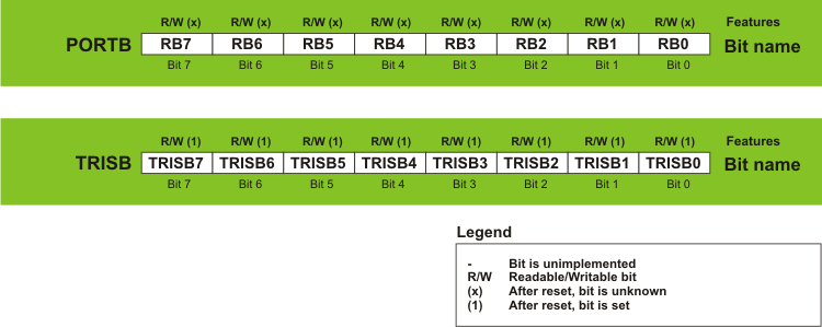
PORTB and TRISB registers
Port PORTB is an 8-bit wide, bidirectional port. Bits of the TRISB register determine the function of its pins.

Similar to port PORTA, a logic one (1) on the TRISB register bit configures the appropriate port PORTB pin as an input and vice versa. Six pins of this port can act as analog inputs (AN). Bits of the ANSELH register determine whether these pins are to be configured as analog inputs or digital inputs/outputs:
RB0 = AN12 (determined by the ANS12 bit of the ANSELH register)
RB1 = AN10 (determined by the ANS10 bit of the ANSELH register)
RB2 = AN8 (determined by the ANS8 bit of the ANSELH register)
RB3 = AN9 (determined by the ANS9 bit of the ANSELH register)
RB4 = AN11 (determined by the ANS11 bit of the ANSELH register)
RB5 = AN13 (determined by the ANS13 bit of the ANSELH register)
Each port PORTB pin is assigned an additional function related to some of the built-in peripheral modules, which will be explained later.
The following features makes this port diffierent from other ports, hence its pins are commonly used:
- All the port PORTB pins have built in pull-up resistors, which makes them ideal for connecting to push buttons (keyboard), switches or optocouplers. In order to connect these resistors to the PORTB pins, the appropriate bit of the WPUB register should be set.*
Having a high resistance (several tens of kiloohms), these ‘virtual’ resistors do not affect pins configured as outputs, but serve as a useful complement when they act as inputs. Otherwise, without these resistors attached the input pins would act as floating due to their high input resistance.
* Apart from the bits of the WPUB register, there is another bit affecting the installation of all pull-up resistors. It is the RBPU bit of the OPTION_REG register.
- Port PORTB can be used as an interrupt source. If enabled, each port PORTB bit configured as an input may cause an interrupt by changing its logic state. In order to enable pins to cause an interrupt, the appropriate bit of the IOCB register should be set.
Owing to these features, the port PORTB pins are commonly used for checking push buttons on the keyboard as they are able to unerringly register any button pressure. There is no need to ‘scan’ these inputs all the time, therefore. When the X, Y and Z pins are configured as outputs set to logic one (1), it is only necessary to wait for an interrupt request to arrive after pressing a button. By combining zeros and ones on these outputs it is checked which push button is pressed. Refer to figure below:
Let's do it in mikroBasic...
'The PORTB.1 pin is configured as a digital input. Any change of its logic state will cause
'an interrupt. It also has a pull-up resistor. All other PORTB pins are digital ... outputs.

ANSEL, ANSELH = 0 ' All I/O pins are configured as digital
PORTB = 0 ' All PORTB pins are cleared
TRISB = %00000010 ' All PORTB pins except PORTB.1 are configured as outputs
OPTION_REG.RBPU = 0 ' Pull-up resistors are enabled
WPUB.1 = 1 ' Pull-up resistor is connected to the PORTB.1 pin
IOCB.1 = 1 ' The PORTB.1 pin may cause an interrupt on logic state change
INTCON.RBIE = 1 ' Interrupt on PORTB change is enabled
INTCON.GIE = 1 ' All unmasked interrupts are enabled
...
PIN RB0/INT
The RB0/INT pin is the only ‘true’ external interrupt source. It can be configured so as to respond to signal raising edge (zero-to-one transition) or signal falling edge (one-to-zero transition). The INTEDG bit of the OPTION_REG register is used as a signal selector.
RB6 AND RB7 PINS
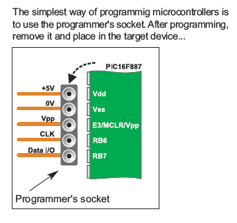
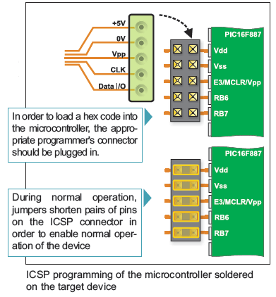
The PIC16F887 is not provided with special pins for programming. Instead, this function is assigned to I/O pins. As a matter of fact, the port PORTB pins are used for clock (RB6) and data transfer (RB7) during programming. In addition, it is necessary to provide the power supply voltage Vdd (5V) as well as the appropriate voltage Vpp (12-14V) for the FLASH memory programming. The MCLR pin is used for this purpose. You don’t have to think of all these details, nor which one of these voltages is to be applied first since the programmer takes care of that. It enables the program to be loaded into the microcontroller even when it is soldered onto the target device. The loaded program can normally be modified in the same manner. This process is called ICSP (In-Circuit Serial Programming). In order to make advantage of this option, it is necessary to plan ahead.
It means that it is necessary to install a miniature 5-pin connector on the target device so as to enable the microcontroller to be provided with necessary programming voltages. In order to prevent these voltages from interfering with the operation of other modules connected to the microcontroller pins, it is necessary to isolate them from the board during the process of programming using resistors or jumpers.


As you can see, voltages applied to the pins on the programmer's socket are the same as those used during the ICSP programming
PORTC and TRISC register
Port PORTC is an 8-bit wide, bidirectional port. Bits of the TRISC register determine the function of its pins. Similar to other ports, a logic one (1) applied to the TRISC register configures the appropriate port PORTC pin as an input.
All additional functions of the port PORTC bits will be described later.
PORTD and TRISD register
Port PORTD is an 8-bit wide, bidirectional port. Bits of the TRISD register determine the function of its pins. A logic one (1) applied to the TRISD register configures the appropriate port PORTD pin as an input.
PORTE and TRISE register
Port PORTE is a 4-bit wide, bidirectional port.
The TRISE register’s bits determine the function of its pins. Similar to other ports, a logic one (1) applied to the TRISE register configures the appropriate port PORTE pin as an input.
The exception is the RE3 pin which is always configured as an input.
Similar to ports PORTA and PORTB, three pins can be configured as analog inputs in this case. The ANSEL register bits determine whether a pin will act as an analog input (AN) or a digital input/output:
RE0 = AN5 (determined by the ANS5 bit of the ANSEL register);
RE1 = AN6 (determined by the ANS6 bit of the ANSEL register); and
RE2 = AN7 (determined by the ANS7 bit of the ANSEL register).
Let's do it in mikroBasic...
' The PORTE.0 pin is configured as an analog input while another three pins of the same
' p.o.r.t are configured as digital.
ANSEL = %00100000 ' The PORTE.0 pin is configured as analog
ANSELH = 0 ' All other I/O pins are configured as digital
TRISE = %00000001 ' All PORTE pins except PORTE.0 are configured as outputs
PORTE = 0 ' All PORTE pins are cleared
...
ANSEL and ANSELH register
The ANSEL and ANSELH registers are used to configure the input mode of an I/O pin as analog or digital.
The rule to follow reads:
To configure a pin as an analog input, the appropriate bit of the ANSEL or ANSELH registers must be set (1). To configure a pin as a digital input/output, the appropriate bit must be cleared (0).
The state of the ANSEL register bits doesn’t affect digital output functions. The result of any attempt to read a port pin configured as an analog input will be 0.

In Short
You will probably never write a program which doesn't use ports, so the effort you make to learn all about them will definately pay off. Also, they seem to be the simplest modules within the microcontroller. This is how they are used:
- When designing a device, select a port to be used by the microcontroller for communication with peripheral modules. If you use only digital inputs/outputs, select any port you want. If you intend to use some of the analog inputs, select the appropriate ports supporting such configuration (AN0-AN13).
- Each port pin may be configured either as an input or an output. Bits of the TRISA, TRISB, TRISC, TRISD and TRISE registers determine how the pins of the following ports PORTA, PORTB, PORTC, PORTD and PORTE will act. As simple as that.
- If you use some of the analog inputs, first it is necessary to set appropriate bits of the ANSEL and ANSELH registers at the beginning of the program.
- If you use switches and push buttons as input signal source, it is recommended to con nect them to the port PORTB pins because they have pull-up resistors connected. The use of these resistors is enabled by the RBPU bit of the OPTION_REG register, whereas individual resistors are enabled by bits of the WPUB register.
- It is usually necessary to respond as soon as input pins change their logic state. It doesn’t mean that you have to write a program to check pins’ logic state all the time. Just connect them to the PORTB pins and enable an interrupt to occur on every voltage change. Bits of the IOCB and INTCON registers are in charge of that.


