1. PIC16F887 Microcontroller - Device Overview
The PIC16F887 is one of the latest products from
Microchip. It features all the components which modern microcontrollers normally have. For its low price, wide range of application, high quality and easy availability, it is an ideal solution in applications such as: the control of different processes in industry, machine control devices, measurement of different values etc. Some of its main features are listed below.
- RISC architecture
- Only 35 instructions to learn
- All single-cycle instructions except branches
- Operating frequency 0-20 MHz
- Precision internal oscillator
- Factory calibrated
- Software selectable frequency range of 8MHz to 31KHz
- Power supply voltage 2.0-5.5V
- Consumption: 220uA (2.0V, 4MHz), 11uA (2.0 V, 32 KHz) 50nA (stand-by mode)
- Power-Saving Sleep Mode
- Brown-out Reset (BOR) with software control option
- 35 input/output pins
- High current source/sink for direct LED drive
- software and individually programmable pull-up resistor
- Interrupt-on-Change pin
- 8K ROM memory in FLASH technology
- Chip can be reprogrammed up to 100.000 times
- In-Circuit Serial Programming Option
- Chip can be programmed even embedded in the target device
- 256 bytes EEPROM memory
- Data can be written more than 1.000.000 times
- 368 bytes RAM memory
- A/D converter:
- 14-channels
- 10-bit resolution
- 3 independent timers/counters
- Watch-dog timer
- Analogue comparator module with
- Two analogue comparators
- Fixed voltage reference (0.6V)
- Programmable on-chip voltage reference
- PWM output steering control
- Enhanced USART module
- Supports RS-485, RS-232 and LIN2.0
- Auto-Baud Detect
- Master Synchronous Serial Port (MSSP)
- supports SPI and I2C mode
Fig. 1-1 PIC16F887 PDIP 40 Microcontroller
Fig. 1-2 PIC16F887 QFN 44 Microcontroller
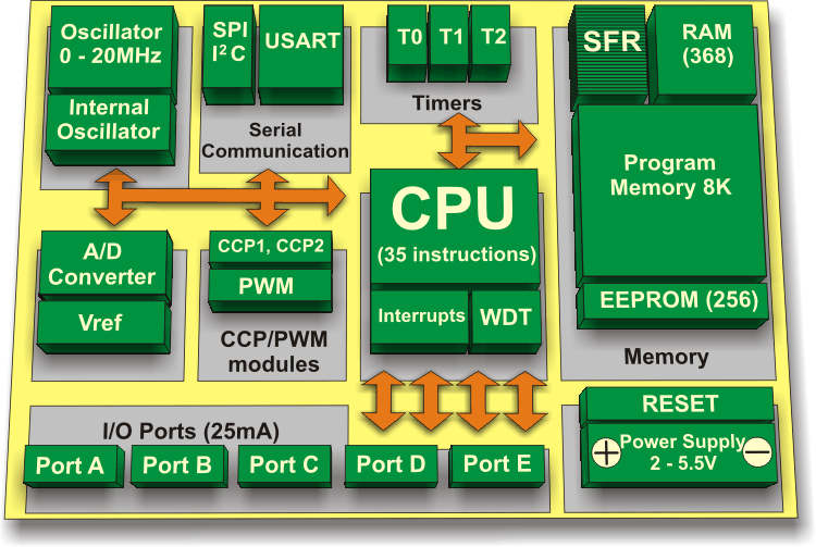
Fig. 1-3 PIC16F887 Block Diagram
Pin Description
As seen in Fig. 1-1 above, the most pins are multi-functional. For example, designator RA3/AN3/Vref+/C1IN+ for the fifth pin specifies the following functions:
- RA3 Port A third digital input/output
- AN3 Third analog input
- Vref+ Positive voltage reference
- C1IN+ Comparator C1positive input
This small trick is often used because it makes the microcontroller package more compact without affecting its functionality. These various pin functions cannot be used simultaneously, but can be changed at any point during operation. The following tables, refer to the PDIP 40 microcontroller.

Table 1-1 Pin Assignment
Table 1-1 cont. Pin Assignment
Table 1-1 cont. Pin Assignment
Central Processor Unit (CPU)
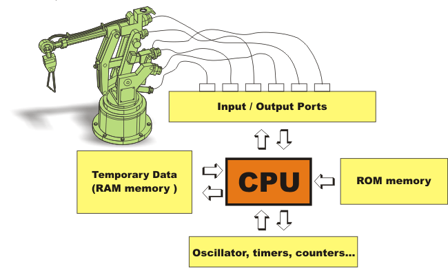
I’m not going to bore you with the operation of the CPU at this stage, however it is important to state that the CPU is manufactured with in RISC technology an important factor when deciding which microprocessor to use. RISC
Reduced Instruction Set Computer, gives the PIC16F887 two great advantages:
- The CPU can recognizes only 35 simple instructions (In order to program some other microcontrollers it is necessary to know more than 200 instructions by heart).
- The execution time is the same for all instructions except two and lasts 4 clock cycles (oscillator frequency is stabilized by a quartz crystal). The Jump and Branch instructions execution time is 2 clock cycles. It means that if the microcontroller’s operating speed is 20MHz, execution time of each instruc tion will be 200nS, i.e. the program will be executed at the speed of 5 million instructions per second!

Fig. 1-4 CPU Memory
Memory
This microcontroller has three types of memory- ROM, RAM and EEPROM. All of them will be separately discussed since each has specific functions, features and organization.
ROM Memory
ROM memory is used to permanently save the program being executed. This is why it is often called “program memory”. The PIC16F887 has 8Kb of ROM (in total of 8192 locations). Since this ROM is made with FLASH technology, its contents can be changed by providing a special programming voltage (13V). Anyway, there is no need to explain it in detail because it is automatically performed by means of a special program on the PC and a simple electronic device called the Programmer.

Fig. 1-5 ROM Memory Consept
EEPROM Memory
Similar to program memory, the contents of EEPROM is permanently saved, even the power goes off. However, unlike ROM, the contents of the EEPROM can be changed during operation of the microcontroller. That is why this memory (256 locations) is a perfect one for permanently saving results created and used during the operation.
RAM Memory
This is the third and the most complex part of microcontroller memory. In this case, it consists of two parts: general-purpose registers and special-function registers (SFR). Even though both groups of registers are cleared when power goes off and even though they are manufactured in the same way and act in the similar way, their functions do not have many things in common.

Fig. 1-6 SFR and General Purpose Registers
General-Purpose Registers
General-Purpose registers are used for storing temporary data and results created during operation. For example, if the program performs a counting (for example, counting products on the assembly line), it is necessary to have a register which stands for what we in everyday life call “sum”. Since the microcontroller is not creative at all, it is necessary to specify the address of some general purpose register and assign it a new function. A simple program to increment the value of this register by 1, after each product passes through a sensor, should be created. Therefore, the microcontroller can execute that program because it now knows what and where the sum which must be incremented is. Similarly to this simple example, each program variable must be preassigned some of general-purpose register.
SFR Registers
Special-Function registers are also RAM memory locations, but unlike general-purpose registers, their purpose is predetermined during manufacturing process and cannot be changed. Since their bits are physically connected to particular circuits on the chip (A/D converter, serial communication module, etc.), any change of their contents directly affects the operation of the microcontroller or some of its circuits. For example, by changing the TRISA register, the function of each port A pin can be changed in a way it acts as input or output. Another feature of these memory locations is that they have their names (registers and their bits), which considerably facilitates program writing. Since high-level programming language can use the list of all registers with their exact addresses, it is enough to specify the register’s name in order to read or change its contents.
RAM Memory Banks
The data memory is partitioned into four banks. Prior to accessing some register during program writing (in order to read or change its contents), it is necessary to select the bank which contains that register. Two bits of the STATUS register are used for bank selecting, which will be discussed later. In order to facilitate operation, the most commonly used SFRs have the same address in all banks which enables them to be easily accessed.

Table 1-2 Address Banks
Table 1-3 SFR Bank 0
Table 1-4 SFR Bank 1
Table 1-5 SFR Bank 2
Table 1-6 SFR Bank 3
STACK
A part of the RAM used for the stack consists of eight 13-bit registers. Before the microcontroller starts to execute a subroutine (
CALLinstruction) or when an interrupt occurs, the address of first next instruction being currently executed is pushed onto the stack, i.e. onto one of its registers. In that way, upon subroutine or interrupt execution, the microcontroller knows from where to continue regular program execution. This address is cleared upon return to the main program because there is no need to save it any longer, and one location of the stack is automatically available for further use. It is important to understand that data is always circularly pushed onto the stack. It means that after the stack has been pushed eight times, the ninth push overwrites the value that was stored with the first push. The tenth push overwrites the second push and so on. Data overwritten in this way is not recoverable. In addition, the programmer cannot access these registers for write or read and there is no Status bit to indicate stack overflow or stack underflow conditions. For that reason, one should take special care of it during program writing.
Interrupt System
The first thing that the microcontroller does when an interrupt request arrives is to execute the current instruction and then stop regular program execution. Immediately after that, the current program memory address is automatically pushed onto the stack and the default address (predefined by the manufacturer) is written to the program counter. That location from where the program continues execution is called the interrupt vector. For the PIC16F887 microcontroller, this address is 0004h. As seen in Fig. 1-7 below, the location containing interrupt vector is passed over during regular program execution. Part of the program being activated when an interrupt request arrives is called the interrupt routine. Its first instruction is located at the interrupt vector. How long this subroutine will be and what it will be like depends on the skills of the programmer as well as the interrupt source itself. Some microcontrollers have more interrupt vectors (every interrupt request has its vector), but in this case there is only one. Consequently, the first part of the interrupt routine consists in interrupt source recognition. Finally, when the interrupt source is recognized and interrupt routine is executed, the microcontroller reaches the
RETFIE instruction, pops the address from the stack and continues program execution from where it left off.

Fig.1-7 Interrupt System
How to use SFRs
You have bought the microcontroller and have a good idea how to use it...There is a long list of SFRs with all bits. Each of them controls some process. All in all, it looks like a big control table with a lot of instruments and switches. Now you are concerned about whether you will manage to learn how to use them all? You will probably not, but don’t worry, you don’t have to! Such powerful microcontrollers are similar to a supermarkets: they offer so many things at low prices and it is only up to you to choose. Therefore, select the field you are interested in and study only what you need to know. Afterwards, when you completely understand hardware operation, study SFRs which are in control of it ( there are usually a few of them). To reiterate, during program writing and prior to changing some bits of these registers, do not forget to select the appropriate bank. This is why they are listed in the tables above.


