Appendix B. Examples
The purpose of this chapter is to provide basic information about microcontrollers that one needs to know in order to be able to use them successfully in practice. This chapter, therefore, does not contain any super interesting program or device schematic with amazing solutions. Instead, the following examples are more proof that program writing is neither a privilege nor a talent issue but the ability of simply putting puzzle pieces together using directives. Rest assured that design and development of devices mainly consists of the following method "test-correct-repeat". Of course, the more you are in it the more complicated it becomes since the puzzle pieces are put together by both children and first-class architects...
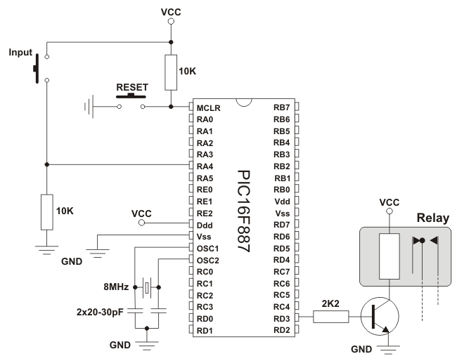
BASIC CONNECTING
As seen in the figure below, in order to enable the microcontroller to operate properly it is necessary to provide:
- Power Supply;
- Reset Signal; and
- Clock Signal.
Clearly, it is about simple circuits, but it does not have to always be like that. If the target device is used for controlling expensive machines or maintaining vital functions, everything gets more and more complicated! However, this solution is sufficient for the time being...
POWER SUPPLY
Even though the PIC16F887 can operate at different supply voltages, why to test "Murphy's low"?! A 5DC power supply is shown above. The circuit, uses a cheap integrated three-terminal positive regulator, LM7805, provides high-quality voltage stability and quite enough current to enable microcontroller and peripheral electronics to operate normally (enough in this case means 1Amp).
RESET SIGNAL
In order that the microcontroller can operate properly, a logic one (VCC) must be applied on the reset pin it explains the connection pin-resistor 10K-VCC. The push-button connecting the reset pin MCLR to GND is not necessary. However, it is almost always provided because it enables the microcontroller safe return to normal operating conditions if something goes wrong. By pushing this button, 0V is brought to the pin, the microcontroller is reset and program execution starts from the beginning. The 10K resistor is there to allow 0V to be applied to the MCLR pin, via the push-button, without shorting the 5VDC rail to ground.
CLOCK SIGNAL
Even though the microcontroller has a built in oscillator, it cannot operate without external components which stabilize its operation and determine its frequency (operating speed of the microcontroller). Depending on which elements are in use as well as their frequencies, the oscillator can be run in four different modes:
- LP - Low Power Crystal;
- XT - Crystal / Resonator;
- HS - High speed Crystal / Resonator; and
- RC - Resistor / Capacitor.
Why are these modes so important? Owing to the fact that it is almost impossible to make a stable oscillator which operates over a wide frequency range, the microcontroller must know which crystal is connected in order that it can adjust the operation of its internal electronics to it. This is why all programs used for chip loading contains an option for oscillator mode selection. See above figure.
Quartz resonator
When a quartz crystal is used for frequency stabilization, the built in oscillator operates at a very precise frequency which is isolated from changes in temperature and voltage power supply as well. This frequency is normally labelled on the microcontroller package.
Apart from the crystal, capacitors C1 and C2 must be also connected as per the schematic below. Their capacitance is not of great importance, therefore, the values provided in the table should be considered as a recommendation rather than a strict rule.
Ceramic resonator
Ceramic resonator is cheaper, but very similar to quartz by its function and the way of operating. This is why the schematics illustrating their connection to the microcontroller are identical. However, the capacitor value is a bit different in this case due to different electric features. Refer to the table.
These oscillators are used when it is not necessary to have extremely precise frequency.
RC oscillator
If the operating frequency is not of importance then there is no need for additional expensive components for stabilization. Instead, a simple RC network, as shown in the figure below, will be enough. Since only the input of the local oscillator input is in use here, the clock signal with frequency Fosc/4 will appear on the OSC2 pin. Furthermore, that frequency becomes operating frequency of the microcontroller, i.e. the speed of instruction execution.
External oscillator
If it is required to synchronize the operation of several microcontrollers or if for some reason it is not possible to use any of the previous schematics, a clock signal may be generated by an external oscillator. Refer to the figure below.
ADDITIONAL COMPONENTS
Regardless of the fact that the microcontroller is a product of modern technology, it is of no use without being connected to additional components. Simply, the appearance of voltage on the microcontroller pins mean nothing if not used for performing certain operations (turn something on/off, shift, display etc.).
This section intentionally covers only the most commonly used additional components in practice such as resistors, transistors, LED diodes, LED displays, LCD displays and RS232 communication circuits.
SWITCHES AND PUSH-BUTTONS
There is nothing simpler than switches and push-buttons! This is definitely the simplest way of detecting the appearance of a voltage on the microcontroller input pin and there is no need for additional explanation of how these components operate. Nevertheless, it is not so simple in practice... Then, what is it all about?

It is about contact bounce- a common problem with mechanical switches. When the contacts strike together, their momentum and elasticity act together to cause bounce. The result is a rapidly pulsed electrical current instead of a clean transition from zero to full current. Generally, it mostly occurs due to vibrations, slight rough spots and dirt between contacts. This effect is usually unnoticeable when using these components in everyday life because the bounce happens too quickly to affect most equipment, but causes problems in some analogue and logic circuits that respond fast enough to misinterpret the on-off pulses as a data stream. Anyway, the whole process does not last long (a few micro- or milliseconds), but long enough to be registered by the microcontroller. When using only a push-button as a pulse counter, errors occurs in almost 100% of cases!
This problem may be easily solved by connecting a simple RC circuit to surpress quick voltage changes. Since the bounce period is not defined, the values of components are not precisely determined. In most cases, it is recommended to use the values as shown in figure below.

If complete stability is needed then radical measures should be taken! The output of the circuit, shown in figure below (RS flip-flop), will change its logic state only after detecting the first pulse triggered by contact bounce. This solution is more expensive (SPDT switch), but the problem is definitely solved!
In addition to these hardware solutions, there is also a simple software solution. When a program tests the state of an input pin and detects a change, the check should be done one more time after a certain delay. If the program confirms the change, it means that a switch/push-button has changed its position. The advantages of such solution are obvious: it is free of charge, effects of noises are eliminated and it can be applied to the poorer quality contacts as well.
RELAY
A relay is an electrical switch that opens and closes under the control of another electrical circuit. It is therefore connected to output pins of the microcontroller and used to turn on/off high-power devices such as motors, transformers, heaters, bulbs, etc. These devices are almost always placed away from the boards sensitive components. There are various types of relays, but all of them operate in the same way. When a current flows through the coil, the relay is operated by an electromagnet to open or close one or many sets of contacts. Similar to optocouplers, there is no galvanic connection (electrical contact) between input and output circuits. Relays usually demand both higher voltage and current to start operation but there are also miniature ones that can be activated by a low current directly obtained from a microcontroller pin.

This figure shows the most commonly used solution.
In order to prevent the appearance of high voltage self-induction caused by a sudden stop of current flow through the coil, an inverted polarized diode is connected in parallel to the coil. The purpose of this diode is to "cut off" the voltage peak.
LED DIODES
You probably know all you need to know about LED diodes, but we should also think of the younger generations...How to destroy a LED?! Well...Very simple.
Quick burning
Like any other diode, LEDs have two ends an anode and a cathode. Connect it properly to a power supply voltage. The diode will happily emit light. Turn it upside down and apply the same power supply voltage (even for a moment). It will not emit light- NEVER AGAIN!
Slow burning
There is a nominal, i.e. maximum current determined for every LED which should not be exceeded. If it happens, the diode will emit more intensive light, but not for a long time!
Something to remember
Similar to the previous example, all you need to do is to discard a current limiting resistor shown below. Depending on power supply voltage, the effect might be spectacular!
LED DISPLAY
Basically, LED display is nothing more than several LEDs moulded in the same plastic case. There are many types of displays composed of several dozens of built in diodes which can display different symbols. The most commonly used is so called 7-segment display. It is composed of 8 LEDs- 7 segments are arranged as a rectangle for symbol displaying and there is an additional segment for decimal point displaying. In order to simplify connection, anodes or cathodes of all diodes are connected to the common pin so that there are common anode displays and common cathode displays, respectively. Segments are marked with the letters from a to g, plus dp, as shown in figure below. On connecting, each diode is treated separately, which means that each must have its own current limiting resistor.
Here are a few important things that one should pay attention to when buying LED displays:
- Depending on whether anodes or cathodes are connected to the common pin, there are common anode displays and common cathode displays. The figure above shows a common anode display. Looking at physical features, there is no difference between these displays at all so it is recommended to check carefully prior installation which of them is in use;
- For each microcontroller pin, there is a maximum current limitation it can receive or give. Because of this, if several displays are connected to the microcontroller it is rec ommended to use so called Low current LEDs using only 2mA for operation; and
- Display segments are usually marked with the letters from a to g, but there is no fast rule indicating to which micro controller pins they should be connected. For this reason it is very important to check connecting prior to commencing program writing or designing a device.
Displays connected to the microcontroller usually occupy a large number of valuable I/O pins, which can be a big problem especially when it is needed to display multi-digital numbers. The problem is more than obvious if, for example, it is needed to display two 6-digit numbers (a simple calculation shows that 96 output pins are needed in this case)! This problem has a solution called MULTIPLEXING.
Here is how an optical illusion based on the same operating principle as a film camera is made. Only one digit at a time is active, but they change their state so quickly that one gets impression that all digits of a number are active simultaneously.

Here is an explanation on the figure above. First a byte representing units is applied on a microcontroller port and a transistor T1 is activated simultaneously. After a while, the transistor T1 is turned off, a byte representing tens is applied on a port and transistor T2 is activated. This process is being cyclically repeated at high speed for all digits and corresponding transistors.
A disappointing fact which indicates that the microcontroller is just a kind of miniature computer designed to understand only the language of zeros and ones is fully expressed when displaying any digit. Namely, the microcontroller does not know what units, tens or hundreds are, nor what ten digits we are used to look like. Therefore, each number to be displayed must go through the following procedure:
First of all, in a particular subroutine a multi-digital number must be split into units, tens etc. Then, these must be stored in special bytes each. Digits get recognizable format by performing "masking". In other words, a binary format of each digit is replaced by a different combination of bits using a simple subroutine. For example, the digit 8 (0000 1000) is replaced by binary number 0111 1111 in order to activate all LEDs displaying digit 8. The only diode remaining inactive in this case is reserved for the decimal point.
If a microcontroller port is connected to the display in a way that bit 0 activates segment "a", bit 1 activates segment "b", bit 2 segment "c" etc., then the table below shows the mask for each digit.

| DIGITS TO DISPLAY |
DISPLAY SEGMENTS |
|
dp |
a |
b |
c |
d |
e |
f |
g |
| 0 |
0 |
1 |
1 |
1 |
1 |
1 |
1 |
0 |
| 1 |
0 |
0 |
1 |
1 |
0 |
0 |
0 |
0 |
| 2 |
0 |
1 |
1 |
0 |
1 |
1 |
0 |
1 |
| 3 |
0 |
1 |
1 |
1 |
1 |
0 |
0 |
1 |
| 4 |
0 |
0 |
1 |
1 |
0 |
0 |
1 |
1 |
| 5 |
0 |
1 |
0 |
1 |
1 |
0 |
1 |
1 |
| 6 |
0 |
1 |
0 |
1 |
1 |
1 |
1 |
1 |
| 7 |
0 |
1 |
1 |
1 |
0 |
0 |
0 |
0 |
| 8 |
0 |
1 |
1 |
1 |
1 |
1 |
1 |
1 |
| 9 |
0 |
1 |
1 |
1 |
1 |
0 |
1 |
1 |
In addition to digits from 0 to 9, there are some letters- A, C, E, J, F, U, H, L, b, c, d, o, r, t- that can be also displayed by means of the appropriate masking.
In the event that the common anode displays are used, all ones contained in the previous table should be replaced by zeros and vice versa. Additionally, NPN transistors should be used as drivers as well.
OPTOCOUPLER
An optocoupler is a device commonly used to galvanically separate microcontroller electronics from any potentially dangerous current or voltage in its surroundings. Optocouplers usually have one, two or four light sources (LED diodes) on their input while on their output, opposite to diodes, there is the same number of elements sensitive to light (phototransistors, photo-thyristors or photo-triacs). The point is that an optocoupler uses a short optical transmission path to transfer a signal between elements of circuit, while keeping them electrically isolated. This isolation makes sense only if diodes and photo-sensitive elements are separately powered. In this way, the microcontroller and expensive additional electronics are completely protected from high voltage and noises which are the most common cause of destroying, damaging or unstable operation of electronic devices in practice. The most frequently used optocouplers are those with phototransistors on their outputs. Additionally, optocouplers with internal base-to-pin 6 connection (there are also optocouplers without it), the base may be left unconnected.

The R/C network represented by the broken line in the figure above denotes optional connection which lessens the effects of noises by eliminating very short pulses.
LCD DISPLAY
This component is specifically manufactured to be used with microcontrollers, which means that it cannot be activated by standard IC circuits. It is used for displaying different messages on a miniature liquid crystal display. The model described here is for its low price and great capabilities most frequently used in practice. It is based on the HD44780 microcontroller (
Hitachi) and can display messages in two lines with 16 characters each. It displays all the letters of alphabet, Greek letters, punctuation marks, mathematical symbols etc. In addition, it is possible to display symbols made up by the user. Other useful features include automatic message shift (left and right), cursor appearance, LED backlight etc.
Along one side of a small printed board there are pins used for connecting to the microcontroller. There are in total of 14 pins marked with numbers (16 if the backlight is built in). Their function is described in the table bellow:
| FUNCTION |
PIN NUMBER |
NAME |
LOGIC STATE |
DESCRIPTION |
| Ground |
1 |
Vss |
- |
0V |
| Power supply |
2 |
Vdd |
- |
+5V |
| Contrast |
3 |
Vee |
- |
0 - Vdd |
| Control of operating |
4 |
RS |
0
1 |
D0 – D7 are interpreted as commands
D0 – D7 are interpreted as data |
| 5 |
R/W |
0
1 |
Write data (from controller to LCD)
Read data (from LCD to controller) |
| 6 |
E |
0
1
From 1 to 0 |
Access to LCD disabled
Normal operating
Data/commands are transferred to LCD |
| Data / commands |
7 |
D0 |
0/1 |
Bit 0 LSB |
| 8 |
D1 |
0/1 |
Bit 1 |
| 9 |
D2 |
0/1 |
Bit 2 |
| 10 |
D3 |
0/1 |
Bit 3 |
| 11 |
D4 |
0/1 |
Bit 4 |
| 12 |
D5 |
0/1 |
Bit 5 |
| 13 |
D6 |
0/1 |
Bit 6 |
| 14 |
D7 |
0/1 |
Bit 7 MSB |
LCD screen
The LCD screen consists of two lines with 16 characters each. Every character consists of 5x8 or 5x11 dot matrix. This book covers the 5x8 character display, which is indeed the most commonly used.
Display contrast depends on the power supply voltage and whether messages are displayed in one or two lines. For this reason, varying voltage 0-Vdd is applied on the pin marked as Vee. Trimmer potentiometer is usually used for that purpose. Some LCD displays have built in backlight (blue or green diodes). When used during operation, a current limiting resistor should be serially connected to one of the pins for backlight (similar to LED diodes).
If there are no characters displayed or if all of them are dimmed when the display is switched on, the first thing that should be done is to check the potentiometer for contrast adjustment. Is it properly adjusted? The same applies if the mode of operation has been changed (writing in one or two lines).
LCD Memory
LCD display contains three memory blocks:
- DDRAM - Display Data RAM;
- CGRAM - Character Generator RAM; and
- CGROM - Character Generator ROM.
DDRAM Memory
DDRAM memory is used for storing characters that should be displayed. The size of this memory is sufficient for storing 80 characters. Some memory locations are directly connected to the characters on display.
It works quite simply: it is enough to configure the display to increment addresses automatically (shift right) and set the starting address for the message that should be displayed (for example 00 hex).
After that, all characters sent through lines D0-D7 will be displayed as a message format we are used to- from left to right. In this very case, displaying starts from the first field of the first line because the address is 00 hex. If more than 16 characters are sent then all of them will be memorized, but only the first sixteen characters will be visible. In order to display the rest of them, a shift command should be used. Virtually, everything looks as if the LCD display is a window which shifts left-right over memory locations containing different characters. In reality, this is how the effect of message shifting on the screen has been created.

If the cursor is on, it appears at the location which is currently addressed. In other words, when a character appears at the cursor position, it will automatically move to the next addressed location.
This is a sort of RAM memory so data can be written to and read from it, but its contents is irretrievably lost upon the power goes off.
CGROM Memory
CGROM memory contains the default character map with all characters that can be displayed on the screen. Each character is assigned to one memory location:

The addresses of CGROM memory locations match the characters of ASCII. If the program being currently executed encounters a command "send character P to port" then the binary value 0101 0000 appears on the port. This value is the ASCII equivalent to the character P. It is then written to LCD, which results in displaying the symbol from the 0101 0000 location of CGROM. In other words, the character "P" is displayed. This applies to all letters of the alphabet (capitals and small), but not to the numbers!
As seen on the previous map, addresses of all digits are pushed forward by 48 relative to their values (digit 0 address is 48, digit 1 address is 49, digit 2 address is 50 etc.). Accordingly, in order to display digits correctly it is necessary to add a decimal number 48 to each of them prior to sending them to LCD.
What is ASCII? From their inception till today, computers can recognize only numbers, but not letters. It means that all data a computer swaps with a peripheral device has a binary format even though the same is recognized by the man as letters (The keyboard is an excellent example)! It’s as simple as that- every character matches the unique combination of zeroes and ones. ASCII is character encoding based on the English alphabet. ASCII code specifies a correspondence between standard character symbols and their numerical equivalents.
LCD Basic Commands
All data transferred to LCD through the outputs D0-D7 will be interpreted as a command or a data, which depends on the pin RS logic state:
RS = 1 - Bits D0 - D7 are addresses of the characters to be displayed. LCD processor addresses one character from the character map and displays it. The DDRAM address specifies the location on which the character is to be displayed. This address is defined prior character transfer or the address of the previously transferred character is automatically incremented.
RS = 0 - Bits D0 - D7 are commands which determine display mode.
The commands recognized by the LCD are listed in table below:
| COMMAND |
RS |
RW |
D7 |
D6 |
D5 |
D4 |
D3 |
D2 |
D1 |
D0 |
EXECUTION TIME |
| Clear display |
0 |
0 |
0 |
0 |
0 |
0 |
0 |
0 |
0 |
1 |
1.64mS |
| Cursor home |
0 |
0 |
0 |
0 |
0 |
0 |
0 |
0 |
1 |
x |
1.64mS |
| Entry mode set |
0 |
0 |
0 |
0 |
0 |
0 |
0 |
1 |
I/D |
S |
40uS |
| Display on/off control |
0 |
0 |
0 |
0 |
0 |
0 |
1 |
D |
U |
B |
40uS |
| Cursor/Display Shift |
0 |
0 |
0 |
0 |
0 |
1 |
D/C |
R/L |
x |
x |
40uS |
| Function set |
0 |
0 |
0 |
0 |
1 |
DL |
N |
F |
x |
x |
40uS |
| Set CGRAM address |
0 |
0 |
0 |
1 |
CGRAM address |
40uS |
| Set DDRAM address |
0 |
0 |
1 |
DDRAM address |
40uS |
| Read "BUSY" flag (BF) |
0 |
1 |
BF |
DDRAM address |
- |
| Write to CGRAM or DDRAM |
1 |
0 |
D7 |
D6 |
D5 |
D4 |
D3 |
D2 |
D1 |
D0 |
40uS |
| Read from CGRAM or DDRAM |
1 |
1 |
D7 |
D6 |
D5 |
D4 |
D3 |
D2 |
D1 |
D0 |
40uS |
I/D 1 = Increment (by 1)         R/L 1 = Shift right
    0 = Decrement (by 1)             0 = Shift left

S 1 = Display shift on           DL 1 = 8-bit interface
  0 = Display shift off             0 = 4-bit interface

D 1 = Display on                 N 1 = Display in two lines
  0 = Display off                  0 = Display in one line

U 1 = Cursor on                  F 1 = Character format 5x10 dots
  0 = Cursor off                   0 = Character format 5x7 dots

B 1 = Cursor blink on            D/C 1 = Display shift
  0 = Cursor blink off               0 = Cursor shift
What is Busy flag ?
Compared to the microcontroller, the LCD is an extremely slow component. Because of this, it was necessary to provide a signal which would, upon command execution, indicate that the display is ready for the next piece of data. That signal, called the
busy flag, can be read from the line D7. When the voltage on this line is 0V (BF=0), the display is ready to receive new data.
LCD Connecting
Depending on how many lines are used for connecting the LCD to the microcontroller, there are 8-bit and 4-bit LCD modes. The appropriate mode is selected at the beginning of the operation in this process called "initialization". 8-bit LCD mode uses outputs D0-D7 to transfer data as explained on the previous page.
The main purpose of 4-bit LED mode is to save valuable I/O pins of the microcontroller. Only 4 higher bits (D4-D7) are used for communication, while others may be unconnected. Each piece of data is sent to the LCD in two steps- four higher bits are sent first (normally through the lines D4-D7) and four lower bits are sent afterwards. Initialization enables the LCD to link and interpret received bits correctly.

Data is rarely read from the LCD (it is mainly transferred from the microcontroller to LCD) so it is often possible to save an extra I/O pin by simple connecting R/W pin to the Ground. Such saving has its price. Messages will be normally displayed, but it will not be possible to read the busy flag since it is not possible to read the display as well. Fortunately, there is a simple solution. After sending a character or a command it is important to give the LCD enough time to do its job. Owing to the fact that the execution of the slowest command lasts for approximately 1.64mS, it will be sufficient to wait approximately 2mS for LCD.
LCD Initialization
The LCD is automatically cleared when powered up. It lasts for approximately 15mS. After this, display is ready for operation. The mode of operation is set by default. It means that:
- Display is cleared.
- Mode
DL = 1 Communication through 8-bit interface
N = 0 Messages are displayed in one line
F = 0 Character font 5 x 8 dots
- Display/Cursor on/off
D = 0 Display off
U = 0 Cursor off
B = 0 Cursor blink off
- Character entry
ID = 1 Displayed addresses are automatically incremented by 1
S = 0 Display shift off
Automatic reset is mostly done without any problems. Mostly, but not always! If for any reason power supply voltage does not reach full value within 10mS, display will start performing completely unpredictably. If voltage supply unit is not able to meet that condition or if it is needed to provide completely safe operation, the process of initialization is applied. Initialization, among other things, causes a new reset enabling display to operate normally.
Refer to the figure below for the procedure on 8-bit initialization:
It is not a mistake! In this algorithm, the same value is transferred three times in a row.
In case of 4-bit initialization, the procedure is as follows:
EXAMPLE 1
Writing header and configuring I/O pins
The only purpose of this program is to turn on a few LED diodes on port B. It is nothing special. Anyway, use this example to study what a real program looks like. The figure below shows a connection scheme, while the program is on the next page.
When switching on, every other LED diode on the port B emits light. That is enough to indicate that the microcontroller is properly connected and operates normally.
This example gives the description of a correctly written header and a few initial directives. They represent a part of the program used in all programs described in this book. To skip repetitiveness, it will not be written in the following examples, but is considered to be at the beginning of every program (marked as a "Header").
The purpose of the header and initial directives is briefly described below.
Header:
The header is placed at the beginning of the program and gives basic information in the form of comments (name of the program, release date etc.). Don't be deluded into thinking that after a few months you will know what that program is about and why it is saved in your computer.
Initial directives:
list p=16f887
This directive defines processor to execute a program.
#include <p16f887.inc>
It enables the compiler to access the document p16f887.inc (If you have MPLAB installed, it is placed by default on C:\Program files\Microchip\MPASM Suite). Every SFR register contained in this document, as well as every bit, has its own name and address. If the program reads for example:
bsf INTCON, GIE
It means that the GIE bit of the INTCON register should be set. Instruction, as such, makes no sense to the compiler. It has to access the ".inc" document in order to know that the seventh bit of the SFR at the address 000B hex should be set.
errorlevel -302
This is a "cosmetic" directive which disables the irritating message "Register in operand not in ..." to appear at the end of every compiling process. It is not necessary, but useful.
__config
This directive is used to include config word in the program upon compiling. It is not necessary because the same operation is performed by software for loading program into chip. However, do you have any idea which software will be used by the end user? What options will be set by default? You are the end user?! Do you know which program you will be using for MCU programming next year? Make life easier for yourself, take this directive as a necessary one and include it in your program.
EXAMPLE 2
Using program loop and internal oscillator LFINTOSC
This is a continuation of the previous example, but deals with a bit more complicated problem... The idea is to make the LED diodes on the port B blink. A simple thing at first glance! It is enough to periodically change logic state on the port B. In this case, numbers 01010101 and 10101010 are selected to change in the following way:
- Set binary combination 01010101 on port B;
- Remain in loop1;
- Replace existing bits combination on port B with 10101010;
- Remain in loop2; and
- Return to the step 1 and repeat the whole procedure.
Do you know how fast this should be done? It would be possible to observe changes on port B only if, apart from the delays provided in loop1 and loop2, the whole process is slowed down approximately 250 times more. Because of this, the microcontroller uses internal oscillator LFINTOSC with the frequency of 31kHz instead of the external oscillator with quartz crystal (8MHz).
You have noticed that the clock signal source has changed "on the fly". If you want to make sure of it, remove quartz crystal prior to switching the microcontroller on. What will happen? The microcontroller will not start operating because the config word loaded with the program requires the use of the crystal on switching on. If you remove the crystal later during the operation, it will not affect the microcontroller at all!
Sorce Code
;************************************************************************
;                    Header
;************************************************************************
;************* DEFINING VARIABLES ***************************************
       cblock  0x20            ; Block of variables starts at address 20h
       counter1                ; Variable "counter1" at address 20h
       endc
;************************************************************************
       org     0x0000          ; Address of the first program instruction

       banksel OSCCON          ; Selects memory bank containing
                               ; register OSCCON
       bcf     OSCCON,6        ; Selects internal oscillator LFINTOSC with
       bcf     OSCCON,5        ; the frequency of 31KHz
       bcf     OSCCON,4
       bsf     OSCCON,0        ; Microcontroller uses internal oscillator

       banksel TRISB           ; Selects bank containing register TRISB
       clrf    TRISB           ; All port B pins are configured as outputs
       banksel PORTB           ; Selects bank containing register PORTB

loop
       movlw   B'01010101'     ; Binary number 01010101 is written to W
       movwf   PORTB           ; Number is moved to PORTB
       movlw   h'FF'           ; Number hFF is moved to W
       movwf   counter1        ; Number is moved to variable "counter1"

loop1
       decfsz  counter1        ; Variable "counter1" is decremented by 1
       goto    loop1           ; If result is 0, continue. If not,
                               ; remain in loop1

       movlw   B'10101010'     ; Binary number 10101010 is moved to W
       movwf   PORTB           ; Number is moved to PORTB
       movlw   h'FF'           ; Number hFF is moved to W
       movwf   counter1        ; Number is moved to variable "counter1"

loop2
       decfsz  counter1        ; Variable "counter1" is decremented by 1
       goto    loop2           ; If result is 0, continue. If not,
                               ; remain in loop2

       goto    loop            ; Go to label loop
       end                     ; End of program
EXAMPLE 3
Using nested loop
The connection scheme is again the same. To make this a bit more interesting, a different combination of port B bits change each other. And, that’s not all of course. As seen from the previous two examples, the microcontroller is very fast and often, it needs to be slowed down. The use of the built-in oscillator LF, as in example 2, is the last measure that should be applied. The problem is more often solved by using nested loops in a program. In this example, the variable "counter1" is decremented 255 times by 1 in the shorter loop1. Prior to leaving this loop, the program will countdown 255 times from 255 to 0. It means that between only two LED diode’s blink on the port, there are 255x255 pulses coming from the quartz oscillator. Precisely speaking, the number of pulses amounts to approximately 196 000 since it also takes some time to execute jump instructions and decrement instructions. Yes, it’s true, the microcontroller mostly waits and does nothing...
Source Code
;******************* Header ***********************************************
;************* DEFINING VARIABLES *****************************************

       cblock      0x20          ; Block of variables starts at address 20h
       counter1                  ; Variable "counter1" at address 20h
       counter2                  ; Variable "counter2" at address 21h
       endc
;**************************************************************************
       org         0x0000        ; Address of the first program instruction

       banksel     TRISB         ; Selects bank containing register TRISB
       clrf        TRISB         ; Clears TRISB

       banksel     PORTB         ; Selects bank containing register PORTB
loop
       movlw       B'11110000'   ; Binary number 11110000 is moved to W
       movwf       PORTB         ; Number is moved to PORTB
       movlw       h'FF'         ; Number hFF is moved to W
       movwf       counter2      ; Number is moved to variable "counter2"

loop2
       movlw       h'FF'         ; Number hFF is moved to W
       movwf       counter1      ; Number is moved to "counter1"
loop1
       decfsz      counter1      ; Decrements "counter1" by 1. If result is 0
       goto        loop1         ; skip next instruction

       decfsz      counter2      ; Decrements "counter2" by 1. If result is 0
       goto        loop2         ; skip next instruction

       movlw       B'00001111'   ; Binary number 00001111 is moved to W
       movwf       PORTB         ; Number is moved to PORTB
       movlw       h'FF'         ; Number hFF is moved to W
       movwf       counter2      ; Number is moved to variable "counter2"

loop4
       movlw       h'FF'         ; Number hFF is moved to W
       movwf       counter1      ; Number is moved to variable "counter1"
loop3
       decfsz      counter1      ; Decrements "counter1" by 1. If result is 0
                                 ; skip next instruction
       goto        loop3
       decfsz      counter2      ; Decrements "counter2" by 1. If result is 0
       goto        loop4         ; skip next instruction
       goto        loop          ; Jump to label loop
       end                       ; End of program
Example 4
Using timer TMR0 and Interrupts
If you have read the previous example, you would have noticed a disadvantage of providing delays using loops. In all these cases, the microcontroller is "captive" and does nothing. It simply waits for some time to pass. Such wasting of time is an unacceptable luxury and some other method should be applied.
Do you remember the story about the timers? About interrupts? This example makes links between them in a practical way. The schematic is still the same as well as the challenge. It is necessary to provide delay long enough to notice changes on a port. This time, the timer TMR0 with the assigned prescaler is used for that purpose. Interrupt occurs on every timer register overflow and interrupt routine increments the number in port B by 1. The whole procedure is performed "behind the scenes" of the whole process, which enables the microcontroller to do other things.
Pay attention to a few details:
- Even though it is unnecessary in this case, the contents of the most important registers (W, STATUS and PCLATH) must be saved at the beginning of the interrupt routine;
- Interrupt causes the appropriate flag bit to be automatically set and the GIE bit to be automatically cleared. At the end of the interrupt routine, do not forget to return these bits to the state they had prior to the interrupt occurring; and
- At the end of the interrupt rutine, important registers should be given the original content.
Source Code
;********************** Header **********************************************
;**************** DEFINING VARIABLES ****************************************

       cblock      0x20            ; Block of variables starts at address 20h
       w_temp                      ; Variable at address 20h
       pclath_temp                 ; Variable at address 21h
       status_temp                 ; Variable at address 22h
       endc

;************************ START OF PROGRAM **********************************
       org         0x0000          ; Address of the first program instruction
       goto        main            ; Go to label "main"

;************************ INTERRUPT ROUTINE *********************************
       org         0x0004          ; Interrupt vector
       movwf       w_temp          ; Saves value in register W
       movf        STATUS          ; Saves value in register STATUS
       movwf       status_temp
       movf        PCLATH          ; Saves value in register PCLATH
       movwf       pclath_temp

       banksel     PORTB           ; Selects bank containing PORTB
       incf        PORTB           ; Increments register PORTB by 1

       banksel     INTCON          ; Selects bank containing INTCON
       bcf         INTCON,TMR0IF   ; Clears interrupt flag TMR0IF

       movf        pclath_temp,w   ; PCLATH is given its original content
       movwf       PCLATH
       movf        status_temp,w   ; STATUS is given its original content
       movwf       STATUS
       swapf       w_temp,f        ; W is given its original content
       swapf       w_temp,w

       bsf         INTCON,GIE      ; Global interrupt enabled
       retfie                      ; Return from interrupt routine

;************************ MAIN PROGRAM **************************************
main                               ; Start of the main program

       banksel     ANSEL           ; Bank containing register ANSEL
       clrf        ANSEL           ; Clears registers ANSEL and ANSELH
       clrf        ANSELH          ; All pins are digital

       banksel     TRISB           ; Selects bank containing register TRISB
       clrf        TRISB           ; All port B pins are configured as outputs

       banksel     OPTION_REG      ; Bank containing register OPTION_REG
       bcf         OPTION_REG,T0CS ; TMR0 counts pulses from oscillator
       bcf         OPTION_REG,PSA  ; Prescaler is assign to timer TMR0

       bsf         OPTION_REG,PS0  ; Prescaler rate is 1:256
       bsf         OPTION_REG,PS1
       bsf         OPTION_REG,PS2

       banksel     INTCON          ; Bank containing register INTCON
       bsf         INTCON,TMR0IE   ; TMR0 interrupt overflow enabled
       bsf         INTCON,GIE      ; Global interrupt enabled

       banksel     PORTB           ; Bank containing register PORTB
       clrf        PORTB           ; Clears port B
loop
       goto        loop            ; Remain here
       end                         ; End of program
Example 5
Using subroutine, using push-buttons
In the previous examples the microcontroller executes the program without being influenced in any way its surrounding. In practice, devices operating in this way are very rare (for example, simple neon signs). You guess, among other components, input pins will also be used in this example. There is a schematic in the figure below, while the program is on the next page. Everything is still very simple.

At the beginning of the program, immediately upon defining variables, the microcontroller pins* are configured by using registers TRISA and TRISB.
In the main program, one bit on port B is set first. Then the contents of this register is constantly moved by one place to the left (instruction rlf PORTB). It gives us the impression that the lit LED diodes is moving. To make it visible, the whole process must be slow enough. Press on the push-button "STOP" stops the movement and the program remains in loop3. Delay is provided by means of a nested loop. This time, it is placed in a short subroutine "DELAY".
* It is not necessary for PORTA pins since they are automatically configured as inputs after every reset.
Source Code
;****************************************************************************
;                    Header
;****************************************************************************
;************* DEFINING VARIABLES *******************************************

       cblock      0x20            ; Block of variables starts at address 20h
       counter1                    ; Variable "counter1" at address 20h
       counter2                    ; Variable "counter2" at address 21h
       endc                        ; Block of variables ends

;************************ MAIN PROGRAM **************************************

       org         0x0000          ; Address of the first program instruction
       banksel     ANSEL           ; Selects bank containing register ANSEL
       clrf        ANSEL           ; Clears registers ANSEL and ANSELH to
       clrf        ANSELH          ; configure all inputs as digital

       banksel     TRISB           ; Selects bank containing register TRISB
       clrf        TRISB           ; All port B pins are configured as outputs
       movlw       B'00000010'
       movwf       TRISA           ; Pin RA1 is input

       banksel     PORTB           ; Selects bank containing register TRISB
       movlw       B'00000001'     ; Writes 1 to register W
       movwf       PORTB           ; Number is moved to PORTB
loop
       rlf         PORTB           ; Port B bits rotates by one place left
       call        DELAY           ; Calls subroutine "DELAY"
loop3
       btfss       PORTA,1         ; Tests the firs port A bit
       goto        loop3           ; "0" is applied to pin.Go to label "loop3"
       goto        loop            ; "1" is applied to pin.Go to label "loop"

;************************ SUBROUTINES ***************************************
DELAY
       clrf        counter2        ; Clears variable "counter2"
loop1
       clrf        counter1        ; Clears variable "counter1"
loop2
       decfsz      counter1        ; Decrements variable "counter1" by 1
       goto        loop2           ; Result is not 0. Go to label loop2
       decfsz      counter2        ; Decrements variable "counter2" by 1
       goto        loop1           ; Result is not 0. Go to lab loop1
       return                      ; Return from subroutine "DELAY"

       end                         ; End of program
EXAMPLE 6
TMR0 as a counter, defining new variables, using relay
This time, TMR0 is used as a counter. The idea is to connect the counter input to one pushbutton so that it counts one pulse at a time upon every button press. When the number of counted pulses becomes equal to the number in register TEST, logic one voltage (5V) will be applied to the PORTD, 3 pin. Since this voltage activates an electro-mechanical relay, this bit is called the same- "Relay".
In this example, the TEST register contains number 5. Naturally, it could be any number and could be calculated or entered via the keyboard. Instead of a relay, the microcontroller can activate some other device and instead of push-buttons it can use sensors. This example illustrates one of the most common uses of the microcontroller in industry. When something is done as many times as needed, then something else should be switched on or off...
Source Code
;****************************************************************************
;                    Header
;****************************************************************************
;************* DEFINING VARIABLES *******************************************

       TEST        equ B'00000101' ; Binary number 00000101 = TEST
       #define     RELAY PORTD,3   ; Pin PORTD,3 = RELAY

;************************ MAIN PROGRAM **************************************

       org         0x0000          ; Address of the first program instruction

       banksel     TRISB           ; Selects bank containing register TRISB
       clrf        TRISB           ; All port B pins are configured as outputs
       clrf        TRISD           ; All port D pins are configured as outputs
       movlw       B'00010000'     ; This number is written to W register
       movwf       TRISA           ; Only the forth pin of port A is input

       banksel     OPTION_REG      ; Bank containing OPTION_REG register
       bsf         OPTION_REG,T0CS ; Pin RA4 is supplied with pulses
       bsf         OPTION_REG,PSA  ; Prescaler rate is 1:1

       banksel     PORTB           ; Selects bank containing PORTB register

       clrf        TMR0            ; Clears timer register
       bcf         PORTD,3         ; Pin PORTD,3 = 0
loop
       movfw       TMR0            ; Timer register is moved to W register
       movwf       PORTB           ; W register is moved to PORTB
       xorlw       TEST            ; Operation exclusive OR between
                                   ; W register and number TEST (00000101)
       btfsc       STATUS,Z        ; If numbers are equal, result is 0 and
       bsf         PORTD,3         ; bit STATUS,Z = 1. Bit PORTD,3 is set
       goto        loop            ; and jump to label loop is executed

       end                         ; End of program
EXAMPLE 7
Using macros in the program, using debounce routine
You have probably noticed in the previous example that the microcontroller does not always operate as expected. Namely, by pressing the push-button, the number on port B is not always incremented by 1. Mechanical push-buttons make several short successive contacts when they have been activated. You guess, the microcontroller registers and counts all that...
There are several ways to solve this problem. This program uses program delay known as
debounce. Basically, it is a simple procedure. Upon input change detection (button press), a short program delay is provided and the program waits for another change (button release). Only after this, the program comes to a conclusion that the button is activated.
In this very case, the push-button is tested by means of macro called
button. Besides, this macro contains a program delay which is provided by means of another macro
pausems.
The main program is relatively simple and enables the variable "cnt" to be incremented and decremented by using two push-buttons. This variable is thereafter copied to port B and affects the LED (logic one (1) turns LED diode on, while logic zero (0) turns LED diode off).
Source Code
;********************** Header **********************
;************* DEFINING VARIABLES *************************

       cblock      0x20            ; Block of variables starts at address 20hex

       HIcnt
       LOcnt
       LOOPcnt
       cnt
       endc                        ; End of block of variables
;**********************************************************************
       ORG         0x000           ; Reset vector
       nop
       goto        main            ; Go to program start (label "main")
;**********************************************************************

       include    "pause.inc"
       include    "button.inc"

;**********************************************************************
main
       banksel      ANSEL          ; Selects bank containing ANSEL
       clrf         ANSEL          ; All pins are digital
       clrf         ANSELH

       banksel      TRISB
       bsf          TRISA, 0
       bsf          TRISA, 1
       clrf         TRISB

       banksel      PORTB
       clrf         cnt
Loop
       button       PORT,0,0,Increment
       button       PORT,1,0,Decrement
       goto         Loop

Increment
       incf         cnt, f
       movf         cnt, w
       movwf        PORTB
       goto         Loop
Decrement
       decf         cnt, f
       movf         cnt, w
       movwf        PORTB
       goto         Loop
       end                         ; End of program
Macro "pausems"
;**********************************************************************
pausems MACRO arg1
       local        Loop1
       local        dechi
       local        Delay1ms
       local        Loop2
       local        End

       movlw        High(arg1)     ; Higher byte of argument is moved
                                   ; to HIcnt
       movwf        HIcnt
       movlw        Low(arg1)      ; Lower byte of argument is moved
                                   ; to LOcnt
       movwf        LOcnt
Loop1
       movf         LOcnt, f       ; Decrements HIcnt and LOcnt while
       btfsc        STATUS, Z      ; needed and calls subroutine Delay1ms

       goto         dechi
       call         Delay1ms
       decf         LOcnt, f
       goto         Loop1
dechi
       movf         HIcnt, f
       btfsc        STATUS, Z
       goto         End
       call         Delay1ms
       decf         HIcnt, f
       decf         LOcnt, f
       goto         Loop1
Delay1ms:                          ; Delay1ms provides delay of
       movlw        .100           ; 100*10us=1ms
       movwf        LOOPcnt        ; LOOPcnt<-100
Loop2:
       nop
       nop
       nop
       nop
       nop
       nop
       nop
       decfsz      LOOPcnt, f
       goto        Loop2           ; Execution time of Loop2
       return                      ; is 10 us
End
       ENDM
;**********************************************************************
Macro "button"
;****************************************************
button MACRO port,pin,hilo,label
       local       Pressed1        ; All labels are local
       local       Pressed2
       local       Exit1
       local       Exit2

       IFNDEF      debouncedelay   ; Enables debounce time to be defined
                                   ; in main program
       #define     debouncedelay .10
       ENDIF

       IF (hilo == 0)              ; If pull-up used
       btfsc       port, pin       ; If "1", push-button is pressed
       goto        Exit1
       pausems     debouncedelay   ; Wait for 10ms debounce
Pressed1
       btfss       port, pin
       goto        Pressed1
       pausems     debouncedelay   ; Wait until released and
       goto        label           ; jump to specified address
Exit1
       ELSE                        ; If pull-down used
       btfss       port, pin
       goto        Exit2           ; If "0", push-button is released
       pausems     debouncedelay   ; Wait for 10ms debounce
Pressed2
       btfsc       port, pin
       goto        Pressed2
       pausems     debouncedelay   ; Wait until released and
       goto        label           ; jump to specified address
Exit2
       ENDIF

       ENDM
;**********************************************************************
EXAMPLE 8
Using timer TMR1 and using interrupt
16-bit timer TMR1 is used in this example. By occupying its registers TMR1L and TMR1H, an interrupt occurs and the number on port B is incremented. This has already been seen in the previous examples. The difference is in the program delay which is a bit longer this time because the prescaler rate is 1:8.
Source Code
;*************************** Header *****************************************
;************* DEFINING VARIABLES *******************************************

       cblock      0x20            ; Block of variables starts at address 20h
       w_temp                      ; Variable at address 20h
       pclath_temp                 ; Variable at address 21h
       status_temp                 ; Variable at address 22h
       endc

;************************ PROGRAM START ************************
       org         0x0000          ; Address of the first program instruction
       goto        main            ; Jump to label "main"

;************************ INTERRUPT ROUTINE **********************************

       org         0x0004          ; Interrupt vector
       movwf       w_temp          ; Save register W

       movf        STATUS          ; Save register STATUS
       movwf       status_temp

       movf        PCLATH          ; Save register PCLATH
       movwf       pclath_temp

       banksel     PORTB           ; Selects bank containing PORTB
       incf        PORTB           ; Register PORTB is incremented by 1

       movf        pclath_temp,w   ; PCLATH is given its original content
       movwf       PCLATH
       movf        status_temp,w   ; STATUS is given its original content
       movwf       STATUS
       swapf       w_temp,f        ; W is given its original content
       swapf       w_temp,w

       banksel     PIR1            ; Selects bank containing PIR1
       bcf         PIR1,TMR1IF     ; Clears interrupt flag TMR1IF

       bsf         INTCON,GIE      ; Global interrupt enabled
       retfie                      ; Return from interrupt routine

;************************ MAIN PROGRAM ***************************************

main                               ; Start of main program
       banksel     ANSEL           ; Selects bank containing register ANSEL
       clrf        ANSEL           ; Clears registers ANSEL and ANSELH
       clrf        ANSELH          ; All pins are digital

       banksel     TRISB           ; Selects bank containing register TRISB
       clrf        TRISB           ; All port B pins are configured as outputs

       banksel     T1CON           ; Selects bank containing register T1CON
       bcf         T1CON,TMR1CS    ; TMR1 counts pulses generated by oscillator

       bsf         T1CON,T1CKPS0   ; Prescaler rate is 1:8
       bsf         T1CON,T1CKPS1
       bsf         T1CON,TMR1ON    ; Turns on timer TMR1

       banksel     PIE1            ; Selects bank containing register PIE1
       bsf         PIE1,TMR1IE     ; TMR1 interrupt overflow enabled
       bsf         INTCON,PEIE     ; Peripheral modules interrupt enabled
                                   ; Timer TMR1 belongs to peripheral modules
       bsf         INTCON,GIE      ; Global interrupt enabled

       banksel     PORTB           ; Selects bank containing register PORTB
       clrf        PORTB           ; Clears port B
loop
       goto        loop            ; Remain here
       end                         ; End of program
EXAMPLE 9
Using timer TMR2, configuring quartz oscillator
This example illustrates the use of timer TMR2. The microcontroller uses internal oscillator HFINTOSC with the frequency of 500 kHz. The whole program works as follows: After the period of time defined by register PR, prescaler and postscaler has expired, an interrupt occurs. Interrupt routine decrements the content of the PR register and simultaneously increments the content of port B. Since the number in register PR, which determines when interrupt is to occur is constantly decremented, interrupt will occur for shorter and shorter periods of time. In other words, counting will be carried out faster. A new cycle of accelerated counting starts after every register PR overflow.
Source Code
;********************** Header ***************************************************
;************* DEFINING VARIABLES ************************************************

       cblock      0x20            ; Block of variables starts at address 20h
       w_temp                      ; Variable at address 20h
       pclath_temp                 ; Variable at address 21h
       status_temp                 ; Variable at address 22h
       endc

;************************ PROGRAM START ******************************************
       org         0x0000          ; Address of the first program instruction
       goto        main            ; Jump to label "main"

;************************ INTERRUPT ROUTINE **************************************

       org         0x0004          ; Interrupt vector
       movwf       w_temp          ; Save register W

       movf        STATUS          ; Save register STATUS
       movwf       status_temp

       movf        PCLATH          ; Save register PCLATH
       movwf       pclath_temp

       banksel     PORTB           ; Selects bank containing PORTB
       incf        PORTB           ; Increments PORTB register by 1
       banksel     PR2             ; Selects bank containing PR2
       decf        PR2             ; PR2 is decremented by 1
       movf        pclath_temp,w   ; PCLATH is given its original state
       movwf       PCLATH
       movf        status_temp,w   ; STATUS is given its original state
       movwf       STATUS
       swapf       w_temp,f        ; W is given its original state
       swapf       w_temp,w

       banksel     PIR1            ; Selects bank containing PIR1
       bcf         PIR1,TMR2IF     ; Clears interrupt flag TMR2IF

       bsf         INTCON,GIE      ; Global interrupt enabled
       retfie                      ; Return from interrupt routine

;************************ MAIN PROGRAM *******************************************
main                               ; Start of the main program
       banksel     OSCCON          ; Selects bank containing register OSCCON
       bcf         OSCCON,6        ; Selects internal oscillator HFINTOSC with
       bsf         OSCCON,5        ; frequency of 500KHz
       bsf         OSCCON,4
       bsf         OSCCON,0        ; Microcontroller uses internal oscillator

       banksel     ANSEL           ; Selects bank containing register ANSEL
       clrf        ANSEL           ; Clears registers ANSEL and ANSELH
       clrf        ANSELH          ; All pins are digital

       banksel     TRISB           ; Selects bank containing register TRISB
       clrf        TRISB           ; All port B pins are configured as outputs
       clrf        PR2

       banksel     T2CON           ; Selects bank containing register T2CON
       movlw       H'FF'           ; Sets all control register bits
       movwf       T2CON           ; prescaler=1:16, postscaler=1:16 TMR2=ON
       clrf        PORTB

       banksel     PIE1            ; Selects bank containing register PIE1
       bsf         PIE1,TMR2IE     ; TMR2 interrupt enabled
       bsf         NTCON,PEIE      ; Peripheral modules interrupt enabled
                                   ; Timer TMR2 belongs to peripheral modules
       bsf         INTCON,GIE      ; Global interrupt enabled
loop
       goto        loop            ; Remain here
       end                         ; End of program
EXAMPLE 10
Module CCP1 as PWM signal generator
Since the CCP modules have a wide range of possibilities they are commonly used in practice. This example illustrates the use of CCP1 module in PWM mode. Bits of the CCP1CON register determine that the module operates as a single-output PWM. The same bits determine the PWM frequency to be 4.88 kHz. To make things more interesting, the duration of the output P1A (PORTC,2) pulses may be changed by means of push-buttons symbolically called "DARK" and "BRIGHT". Push-buttons are tested in interrupt routine initiated by the timer TMR1. Any change affects the LED diode so that it changes light intensity. Note that port B does not use external resistors because internal pull-up resistors are enabled. The whole process of generating PWM signal is performed "behind the scenes", which enables the microcontroller to do other things.
Source Code
;********************** Header **********************************************
;************* DEFINING VARIABLES *******************************************
      cblock       0x20            ; Block of variables starts at address 20h
      w_temp                       ; Variable at address 20h
      pclath_temp                  ; Variable at address 21h
      status_temp                  ; Variable at address 22h
      endc

      #define      DARK PORTB,0    ; Push-button "DARK" is connected
                                   ; to PORTB,0 pin
      #define      BRIGHT PORTB,1  ; Push-button "BRIGHT" is connected
                                   ; to PORTB,1 pin
;************************ PROGRAM START *************************************

      org          0x0000          ; First program instruction address
      goto         main            ; Jump to label "main"

;************************ INTERRUPT ROUTINE *********************************

      org          0x0004          ; Interrupt vector

      movwf        w_temp          ; Save register W

      movf         STATUS          ; Save register STATUS
      movwf        status_temp

      movf         PCLATH          ; Save register PCLATH
      movwf        pclath_temp

      banksel      CCPR1L
      btfss        DARK            ; Tests push-button "DARK"
      decf         CCPR1L          ; Push-button is pressed - decrement CCP1L by 1
      btfss        BRIGHT          ; Testing push-button "BRIGHT"
      incf         CCPR1L          ; Push-button is pressed - increment CCP1L by 1

      movf         pclath_temp,w   ; PCLATH is given its original content
      movwf        PCLATH
      movf         status_temp,w   ; STATUS is given its original content
      movwf        STATUS
      swapf        w_temp,f        ; W is given its original content
      swapf        w_temp,w

      banksel      PIR1            ; Selects bank containing PIR1
      bcf          PIR1,TMR1IF     ; Clears interrupt flag TMR1IF

      bsf          TMR1H,7         ; Accelerates timer TMR0 counting
      bsf          TMR1H,6         ;
      bsf          INTCON,GIE      ; Global interrupt enabled
      retfie                       ; Return from interrupt routine

;************************ MAIN PROGRAM **************************************

main                               ; Start of the main program
      banksel      ANSEL           ; Selects bank containing register ANSEL
      clrf         ANSEL           ; Clears registers ANSEL and ANSELH
      clrf         ANSELH          ; All pins are digital

      banksel      OPTION_REG      ; Selects bank containing register ANSEL
      bcf          OPTION_REG,7    ; Pull-up resistors enabled
      bsf          WPUB,0          ; Pull-up resistors enabled
      bsf          WPUB,1          ; on port B pins 0 and 1

      banksel      TRISC           ; Selects bank containing register TRISC
      clrf         TRISC           ; All port C pins are configured as outputs

      banksel       T1CON          ; Selects bank containing register T1CON
      bcf           T1CON,TMR1CS   ; TMR1 operates as a timer
      bcf           T1CON,T1CKPS0  ; Prescaler rate is 1:8
      bcf           T1CON,T1CKPS1
      bsf           T1CON,TMR1ON   ; Activates timer TMR1

      banksel       PIE1           ; Selects bank containing register PIE1
      bsf           PIE1,TMR1IE    ; Interrupt TMR1 is enabled
      bsf           INTCON,PEIE    ; Peripheral modules interrupts are
                                   ; enabled
      bsf           INTCON,GIE     ; Global interrupt enabled

      movlw         B'11111101'    ; Prescaler TMR2 = 1:4
      banksel       T2CON
      movwf         T2CON
      movlw         B'11111111'    ; Number in register PR2
      banksel       PR2
      movwf         PR2

      banksel       CCP1CON
      movlw         B'00001100'    ; Bits to configure CCP1 module
      movwf         CCP1CON
loop
      goto          loop           ; Remain here
      end                          ; End of program
EXAMPLE 11
Using A/D converter
PIC16F887 A/D converter is used in this example. Everything is quite simple. A variable analog signal is applied on the AN2 pin while the result of conversion is shown on port B as a binary number. In order to simplify the program as much as possible, only 8 lower bits of the result of conversion are shown. GND is used as a negative voltage reference Vref-, while positive voltage reference is applied on the AN3 pin. It enables voltage measurement scale to "stretch and shrink".
To make this clear, the A/D converter always generates a 10-bit binary result, which means that it detects a total of 1024 voltage levels (210=1024). The difference between two voltage levels is not always the same. The less the difference between Vref+ and Vref, the less the difference will be between two of 1024 levels. Accordingly, the A/D converter is able to detect slight changes in voltage.
Source Code
;*********************** Header *********************************************
;************************ PROGRAM START *************************************

       org         0x0000          ; Address of the first program instruction

       banksel     TRISB           ; Selects bank containing register TRISB
       clrf        TRISB           ; All port B pins are configured as outputs
       movlw       B'00001100'
       movwf       TRISA           ; Pins RA2 and RA3 are configured as inputs

       banksel     ANSEL           ; Selects bank containing register ANSEL
       movlw       B'00001100'     ; Inputs AN2 and AN3 are analog while
       movwf       ANSEL           ; all other pins are digital
       clrf        ANSELH

       banksel     ADCON1          ; Selects bank including register ADCON1
       bsf         ADCON1,ADFM     ; Right justification of result
       bcf         ADCON1,VCFG1    ; Voltage Vss is used as Vref
       bsf         ADCON1,VCFG0    ; RA3 pin voltage is used as Vref+

       banksel     ADCON0          ; Selects bank containing register ADCON0
       movlw       B'00001001'     ; AD converter uses clock Fosc/2, AD channel
       movwf       ADCON0          ; on RA2 pin is used for conversion and
                                   ; AD converter is enabled
loop
       banksel     ADCON0
       btfsc       ADCON0,1        ; Tests bit GO/DONE
       goto        loop            ; Conversion in progress, remain in
                                   ; loop
       banksel     ADRESL
       movf        ADRESL,w        ; Lower byte of conversion result is
                                   ; copied to W
       banksel     PORTB
       movwf       PORTB           ; Byte is copied to PORTB
       bsf         ADCON0,1        ; Starts new conversion
       goto        loop            ; Jump to label "loop"
       end                         ; End of program
EXAMPLE 12
Using EEPROM memory
This example demonstrates write to and read from built-in EEPROM memory. The program works as follows. The main loop constantly reads EEPROM memory location at address 5 (decimal). This number is displayed on port D. The same loop tests the state of three push-buttons connected to port A. The push-buttons "INCREMENT" and "DECREMENT" have the same purpose like in example 7 - increment and decrement the variable "cnt" which is thereafter displayed on port B. The push-button "MEMO" enables that variable to be written to EEPROM memory. In order to check it, it is enough to press this push-button and switch off the device. On the next switch on, the program displays the value of the variable on port D (at the moment of writing, this value was displayed on port B).
Source Code
;********************** Header **********************************************
;*********** Defining variables in program **********************************
       cblock      0x20            ; Block of variables starts at address 20h

       HIcnt
       LOcnt
       LOOPcnt
       cnt
       endc                        ; End of block

;****************************************************************************
       ORG         0x000           ; Reset vector
       nop
       goto        main            ; Go to start of the program (label "main")
;****************************************************************************
       include     "pause.inc"
       include     "button.inc"
;****************************************************************************
main
       banksel     ANSEL           ; Selects bank containing ANSEL
       clrf        ANSEL
       clrf        ANSELH          ; All pins are digital

       banksel     TRISB
       bsf         TRISA, 0        ; Input pin
       bsf         TRISA, 1        ; Input pin
       bsf         TRISA, 2        ; Input pin
       clrf        TRISB           ; All port B pins are outputs
       clrf        TRISD           ; All port D pins are outputs
       banksel     PORTB
       clrf        PORTB           ; PORTB=0
       clrf        PORTD           ; PORTD=0
       clrf        cnt             ; cnt=0
Loop
       banksel     PORTA
       button      PORTA,0,0,Increment
       button      PORTA,1,0,Decrement
       button      PORTA,2,0,Save

       banksel     EEADR
       movlw       .5              ; Reads EEPROM memory location
       movwf       EEADR           ; at address 5
       banksel     EECON1
       bcf         EECON1,EEPGD
       bsf         EECON1,RD       ; Reads data from EEPROM memory
       banksel     EEDATA
       movfw       EEDATA          ; Moves data to W
       banksel     PORTD
       movwf       PORTD           ; Data is moved from W to PORTD
       goto        Loop
Increment                          ; Increments number on port B
       incf        cnt, f
       movf        cnt, w
       movwf       PORTB
       goto        Loop
Decrement                          ; Decrements number on port B
       decf        cnt, f
       movf        cnt, w
       movwf       PORTB
       goto        Loop
Save                               ; Copies data from port B to EEPROM
       banksel     EEADR           ; memory location at address 5
       movlw       .5
       movwf       EEADR           ; Writes address
       banksel     PORTB
       movfw       PORTB           ; Copies port B to register W
       banksel     EEDAT
       movwf       EEDAT           ; Writes data to temporary register
       banksel     EECON1
       bcf         EECON1,EEPGD
       bsf         EECON1,WREN     ; Write enabled

       bcf         INTCON,GIE      ; All interrupts disabled
       btfsc       INTCON,GIE
       goto        $-2

       movlw       55h
       movwf       EECON2
       movlw       H'AA'
       movwf       EECON2
       bsf         EECON1,WR

       btfsc       EECON1,WR       ; Wait for write to complete
       goto        $-1

       bsf         INTCON,GIE      ; Interrupt enabled
       bcf         EECON1,WREN
       goto        Loop            ; Tests push-buttons again
       end                         ; End of program
EXAMPLE 13
Two-digit LED counter, multiplexing
In this example, the microcontroller operates as a two-digit counter. Concretely, the variable Dval is decremented (slow enough to be visible) and its value is displayed on twodigit LED display (99-0). The challenge is to enable binary number to be converted in decimal one and split it in two digits (tens and ones). Besides, since the LED display segments are connected in parallel, it is necessary to ensure that they change fast in order to make impression of simultaneous light emission (time-division multiplexing). Remember that in electronics, multiplexing allows several analog signals to be processed by one analog-todigital converter (ADC). In this very case, time-division multiplexing is performed by the timer TMR0, while binary to decimal number conversion is performed in macro "digbyte". Counter may be reset to its starting value (99) at any moment by pressing the pushbutton "COUNTER RESET".
Source Code
;************************* Header *******************************************
;****************************************************************************
;                   DEFINING VARIABLES IN PROGRAM
       w_temp      EQU 0x7D        ; Variable for saving W register

       status_temp EQU 0x7E        ; Variable for saving STATUS register

       pclath_temp EQU 0x7F        ; Variable for saving PCLATH register

       CBLOCK      0x20            ; Block of variables starts at address 20h

       Digtemp
       Dig0                        ; Variables for displaying digits - LSB
       Dig1
       Dig2
       Dig3                        ; Variables for displaying digits - MSB
       Dval                        ; Counter value
       One                         ; Auxiliary variable which determines which
                                   ; display is to be switched on

       ENDC                        ; End of block of variables

       poc_vr      EQU .99         ; Initial  counter value is 99

       include     "Digbyte.inc"

;****************************************************************************
       ORG         0x0000          ; First instruction address
       goto        main            ; Jump to label "main"
;****************************************************************************
       ORG         0x0004          ; Interrupt vector address

       movwf       w_temp          ; Move w register to w_temp register


       movf        STATUS,w        ; Move STATUS register to status_temp
       movwf       status_temp     ; register

       movf        PCLATH,w        ; Move PCLATH register to pclath_temp
       movwf       pclath_temp     ; register

       ; Start of interrupt routine...

       BANKSEL     TMR0
       movlw       .100
       movwf       TMR0
       bcf         INTCON, T0IF

       bcf         PORTA, 0
       bcf         PORTA, 1
       btfsc       One, 0
       goto        Lsdon
       goto        Msdon

Lsdon
       incf        One, f
       movlw       HIGH (Bcdto7seg)
       movwf       PCLATH
       digbyte     Dval
       movf        Dig1, w
       call        Bcdto7seg       ; Place L1 mask on the PORTD
       movwf       PORTD
       bsf         PORTA, 1
       goto        ISR_end

Msdon
       incf        One, f
       movlw       HIGH (Bcdto7seg)
       movwf       PCLATH
       digbyte     Dval
       movf        Dig0, w
       call        Bcdto7seg       ; Place LO mask on the PORTD
       movwf       PORTD
       bsf         PORTA, 0
       goto        ISR_end

       ; End of interrupt routine...

ISR_end
       movf        pclath_temp,w   ; PCLATH register is given its original
       movwf       PCLATH          ; state

       movf        status_temp,w   ; STATUS register is given its original
       movwf       STATUS          ; state

       swapf       w_temp,f        ; W register is given its original
                                   ; state
       swapf       w_temp,w
       retfie                      ; Return from interrupt routine
main
       banksel     ANSEL           ; Selects bank containing ANSEL
       clrf        ANSEL           ; All pins are digital
       clrf        ANSELH

       BANKSEL     TRISA
       movlw       b'11111100'     ; RA0 and RA1 are configured as outputs and
                                   ; used for 7-segment display multiplexing
                                   ; RA2 is input push-button for initializa
                                   ; tion

       movwf       TRISA
       clrf        TRISD

       BANKSEL     OPTION_REG
       movlw       b'10000110'     ; TMR0 is incremented each 32us (Fclk=8MHz)
       movwf       OPTION_REG

       BANKSEL     PORTA
       movlw       poc_vr
       movwf       Dval            ; Dval contains counter value
       movlw       b'00000001'     ; Initializes variable specifying display
       movwf       One             ; to switch on
       movwf       PORTA
       movlw       .100
       movwf       TMR0            ; TMR0 interrupt appr.every 10ms
       bsf         INTCON, GIE     ; Global interrupt enabled
       bsf         INTCON, T0IE    ; Timer TMR0 interrupt enabled
       bcf         INTCON, T0IF
Loop
       btfss       One, 3          ; Falling edge encountered?
       goto Dec                    ; Yes! Go to Dec
       btfss       PORTA, 2        ; Counter reset button pressed?
       goto        Reset           ; Yes! Go to Reset
       goto        Loop
       ; Decrement Dval counter by 1
Dec
       btfss       One, 3
       goto        Dec
       movf        Dval, f
       btfsc       STATUS, Z       ; Is Dval equal to 0?
       goto        Loop            ; If it is, go to loop and wait for T2
       decf        Dval, f         ; If Dval not equal to 0, decrement it by 1
       goto        Loop
Reset
       btfss       PORTA, 2        ; Wait for rising edge
       goto        Reset
       movlw       poc_vr
       movwf       Dval            ; Write initial value to counter
       goto        Loop
;****************************************************************************
       ORG         0x0300          ; Lookup table is at the top of third page, but
                                   ; can be placed at some other place, it is impor
                                   ; tant to have it all on one page
Bcdto7seg
       addwf       PCL, f
       DT          0x3f, 0x06, 0x5b, 0x4f, 0x66, 0x6d, 0x7d, 0x07, 0x7f, 0x6f
;****************************************************************************
       END         ; End of program
Macro "digbyte":
digbyte MACRO arg0
       LOCAL       Exit0
       LOCAL       Exit1
       LOCAL       Exit2

       clrf        Dig0
       clrf        Dig1
       clrf        Dig2
       clrf        Dig3

       movf        arg0, w
       movwf       Digtemp
       movlw       .100
Exit2
       incf        Dig2, f
       subwf       Digtemp, f
       btfsc       STATUS, C
       goto        Exit2
       decf        Dig2, f
       addwf       Digtemp, f
Exit1
       movlw       .10
       incf        Dig1, f
       subwf       Digtemp, f
       btfsc       STATUS, C
       goto        Exit1
       decf        Dig1, f
       addwf       Digtemp, f
Exit0
       movf        Digtemp, w
       movwf       Dig0
       ENDM
Macro digbyte is used to convert the number from digital to decimal format. Besides, digits of such decimal number are stored into special registers in order to enable them to be displayed on LED displays.
EXAMPLE 14
Sound generating, using macros
The generation of sound is a task commonly assigned to the microcontroller. Basically, it all comes to generating a pulse sequence on one output pin. While doing so, the proportion of logic zero (0) to logic one (1) duration determines the tone pitch and by changing different tones, different melodies arise.
In this example, any press on push-buttons T1 and T2 generates a sound. The appropriate instructions are stored in macro "beep" containing two arguments.
Source Code
;*********************** Header ***************************************
;******************* Defining variables in program ********************
       cblock      0x20
       HIcnt                       ; Auxiliary variables for macro pausems
       LOcnt
       LOOPcnt
       PRESCwait
       Beep_TEMP1                  ; Belongs to macro "BEEP"
       Beep_TEMP2
       Beep_TEMP3
       endc

#define  BEEPport PORTD, 2         ; Speaker pin
#define  BEEPtris TRISD, 2

       expand

;**********************************************************************
       ORG         0x0000          ; RESET vector address
       goto        main            ; Jump to program start (label - main)
;**********************************************************************
; remaining code goes here

       include     "pause.inc"
       include     "button.inc"
       include     "beep.inc"
main
       banksel     ANSEL           ; Selects bank containing ANSEL
       clrf        ANSEL           ; All outputs are digital
       clrf        ANSELH

       banksel     TRISD
       movlw       b'11111011'     ; PORTA D initialization
       movwf       TRISD
       banksel     PORTD
       BEEPinit                    ; Macro "Beep"
Loop
       button      PORTD,0,0,Play1 ; Push-button 1
       button      PORTD,1,0,Play2 ; Push-button 2
       goto        Loop

Play1                              ; First tone
       BEEP        0xFF, 0x02
       BEEP        0x90, 0x05
       BEEP        0xC0, 0x03
       BEEP        0xFF, 0x03
       goto        Loop

Play2                              ; Second tone
       BEEP        0xBB, 0x02
       BEEP        0x87, 0x05
       BEEP        0xA2, 0x03
       BEEP        0x98, 0x03
       goto        Loop
;**********************************************************************
       END                         ; End of program
Macro "beep":
BEEPinit    MACRO
       bcf         STATUS, RP0
       bcf         STATUS, RP1
       bcf         BEEPport
       bsf         STATUS, RP0
       bcf         STATUS, RP1
       bcf         BEEPtris
       movlw       b'00000111'     ; TMR0 prescaler rate 1:256
       movwf       OPTION_REG      ; OPTION <- W
       bcf         STATUS, RP0
       bcf         STATUS, RP1
       ENDM
BEEP   MACRO       freq, duration
       bcf         STATUS, RP0
       bcf         STATUS, RP1
       movlw       freq
       movwf       Beep_TEMP1
       movlw       duration
       movwf       Beep_TEMP2
       call        BEEPsub
       ENDM
;**********************************************************************
; Subroutines

BEEPsub
       clrf        TMR0            ; Counter initialization
       bcf         INTCON, T0IF
       bcf         BEEPport
BEEPa
       bcf         INTCON, T0IF    ; Clears TMR0 Overflow Flag
BEEPb
       bsf         BEEPport
       call        B_Wait          ; Logic one "1" duration
       bcf         BEEPport
       call        B_Wait          ; Logic zero "0" duration
       btfss       INTCON, T0IF    ; Check TMR0 Overflow Flag,
       goto        BEEPb           ; skip next if set
       decfsz      Beep_TEMP2, f   ; Is Beep_TEMP2 = 0 ?
       goto BEEPa                  ; Go to BEEPa again
       return
B_Wait
       movf Beep_TEMP1, w
       movwf Beep_TEMP3
B_Waita
       decfsz Beep_TEMP3, f
       goto B_Waita
       return
EXAMPLE 15
Using LCD display
This example illustrates the use of the alphanumeric LCD display. The program itself is very simple because macros are used (usually the effort of creating Macros pays off in the end).
Two messages written on two lines change on display. The second message is intended to display the current temperature. Since no sensor is installed, the measurement is not really carried out, the variable "temp" appears on the display instead of the measured temperature.
In reality, the current temperature or some other measured value would be displayed.
Source Code
;*********************** Header ***********************************
                  ; DEFINING VARIABLES IN PROGRAM

       CBLOCK      0x20            ; Block of variables starts at address 20h

       HIcnt                       ; Belongs to macro "pausems"
       LOcnt
       LOOPcnt

       LCDbuf                      ; Belongs to functions "LCDxxx"
       LCDtemp
       LCDportBuf                  ; LCD Port Buffer

       Digtemp                     ; Belongs to macro "digbyte"
       Dig0
       Dig1
       Dig2
       Dig3

       temp
       ENDC                        ; End of block

LCDport   EQU PORTB   ; LCD is on PORTB (4 data lines on RB0-RB3)
RS        EQU 4       ; RS line connected to RB4
EN        EQU 5       ; EN line connected to RB5

;**********************************************************************
       ORG         0x0000          ; Reset vector address
       nop
       goto        main            ; Go to beginning of the program (label "main")
;**********************************************************************
       include    "LCD.inc"
       include    "digbyte.inc"
       include    "pause.inc"
;**********************************************************************
main
       banksel     ANSEL           ; Selects bank containing ANSEL
       clrf        ANSEL           ; All pins are digital
       clrf        ANSELH

       bcf         STATUS,RP0      ; Bank0 active only
       bcf         STATUS,RP1
       movlw       .23
       movwf       temp            ; Move arbitrary value to variable
                                   ; is to be displayed on LCD
       lcdinit                     ; LCD initialization
Loop
       lcdcmd      0x01            ; Instruction to clear LCD
       lcdtext     1, "mikroelektronika" ; Write text from the begin
                                           ; ning of the first line
       lcdtext     2, "Beograd"  ; Write text from the beginning of
                                   ; the second line
       pausems     .2000           ; 2 sec. delay
       lcdcmd      0x01            ; Instruction to clear LCD
       lcdtext 1, "Temperatura1" ; Write text from the begin
                                   ; ning of the first line
       lcdtext 2, "temp=" ; Write text from the beginning of
                            ; the second line
       lcdbyte     temp            ; Write variable (dec.)
       lcdtext 0, " C"           ; Write text after cursor
       pausems     .2000           ; 2 sec. delay
       goto        Loop
;**********************************************************************
       end                         ; End of program
LCD.inc
;**********************************************************************
; Initialization must be done by using macro lcdinit before access
; ing LCD
;**********************************************************************
lcdinit    MACRO
       bcf         STATUS, RP0     ; Bank0
       bcf         STATUS, RP1
       clrf        LCDportBuf
       movf        LCDportBuf, w
       movwf       LCDport
       bsf         STATUS, RP0     ; Bank1
       bcf         STATUS, RP1
       clrf        TRISB           ; LCDport with output LCD
       bcf         STATUS, RP0     ; Bank0
       bcf         STATUS, RP1

; Function set (4-bit mode change)
       movlw       b'00100000'
       movwf       LCDbuf
       swapf       LCDbuf, w
       movwf       LCDportBuf
       bcf         LCDportBuf, RS
       movf        LCDportBuf, w
       movwf       LCDport
       bsf         LCDportBuf, EN
       movf        LCDportBuf, w
       movwf       LCDport
       bcf         LCDportBuf, EN
       movf        LCDportBuf, w
       movwf       LCDport
       call        Delay1ms        ; 1 ms delay

; Function set (display mode set)
       lcdcmd      b'00101100'
       call        Delay1ms        ; 1 ms delay

; Display ON/OFF Control
       lcdcmd      b'00001100'
       call        Delay1ms        ; 1 ms delay

; Entry Mode Set
       lcdcmd      b'00000110'
       call        Delay1ms        ; 1 ms delay

; Display Clear
       lcdcmd      b'00000001'
       pausems     .40             ; 40 ms delay

       ENDM

;**********************************************************************
; lcdcmd sends command to LCD (see the table on the previous page)
; lcdclr is the same as lcdcmd 0x01
;**********************************************************************
lcdcmd MACRO LCDcommand         ; Send command to LCD
       movlw       LCDcommand
       call        LCDcomd
       ENDM

LCDcomd
       movwf       LCDbuf
       bcf         LCDportBuf, RS
       movf        LCDportBuf, w
       movwf       LCDport
       goto        LCDwr
LCDdata
       movwf       LCDbuf
       bsf         LCDportBuf, RS
       movf        LCDportBuf, w
       movwf       LCDport
       goto        LCDwr
LCDwr
       swapf       LCDbuf, w
       call        SendW
       movf        LCDbuf, w
       call        SendW
       return
SendW
       andlw       0x0F
       movwf       LCDtemp

       movlw       0xF0
       andwf       LCDportBuf, f
       movf        LCDtemp, w
       iorwf       LCDportBuf, f
       movf        LCDportBuf, w
       movwf       LCDport
       call        Delay1ms
       bsf         LCDportBuf, EN
       movf        LCDportBuf, w
       movwf       LCDport
       bcf         LCDportBuf, EN
       movf        LCDportBuf, w
       movwf       LCDport
       call        Delay1ms
       return

;**********************************************************************
; lcdtext writes text containing 16 characters which represents a
; macro argument. The first argument select selects the line in which
; text writing is to start. If select is 0, text writing starts from
; cursor current position.
;**********************************************************************
lcdtext    MACRO select, text      ; This macro writes text from cursor
                                   ; current position. Text is specified
                                   ; in argument consisting of 16 charac
                                   ; ters
       local       Message
       local       Start
       local       Exit
       local       i=0
       goto        Start
       Message     DT text         ; Create lookup table from arguments
       DT          0
Start
       IF (select == 1)
       lcdcmd b'10000000'
       ELSE
       IF (select == 2)
       lcdcmd b'11000000'
       ENDIF
       ENDIF

       WHILE (i<16)                ; Repeat conditional program compiling 16 times
       call Message+i              ; Read lookup table and place value in W
       addlw 0
       bz Exit                     ; until 0 is read
       call LCDdata                ; Call routine displaying W on LCD
       i=i+1
       ENDW
Exit
       ENDM

;**********************************************************************
; This macro writes value in size of 1 byte on LCD
; excluding leading zeros
;**********************************************************************
lcdbyte    MACRO arg0
       digbyte     arg0            ; A hundred is in Dig2,
                                   ; A ten is in Dig1 and one in Dig0
       movf        Dig2, w
       addlw       0x30
       call        LCDdata
       movf        Dig1, w         ; If digit is 0 move cursor
       addlw       0x30
       call        LCDdata
       movf        Dig0, w         ; If digit is 0 move cursor
       addlw       0x30
       call        LCDdata
       ENDM
;**********************************************************************
; 1ms Delay
Delay1ms:
       movlw       .200
       movwf       LOOPcnt
Delay10us:
       nop                         ;1us
       nop                         ;1us
       nop                         ;1us
       nop                         ;1us
       nop                         ;1us
       nop                         ;1us
       nop                         ;1us
       decfsz      LOOPcnt, f      ;1us
       goto        Delay10us       ;2us

       return
EXAMPLE 16
RS232 serial communication
This example illustrates the use of the microcontroller's EUSART module. Connection to the PC is enabled through RS232 standard. The program works in the following way: Every byte received via the serial communication is displayed using LED diodes connected to port B and is automatically returned to the transmitter thereafter. If an error occurs on receive, it will be signalled by switching the LED diode on. The easiest way to test device operation in practice is by using a standard Windows program called
Hyper Terminal.
Source Code
;*********************** Header ***************************************
;                  DEFINING VARIABLES IN PROGRAM

       w_temp      EQU 0x7D        ; Variable for saving W register
       status_temp EQU 0x7E        ; Variable for saving STATUS register
       pclath_temp EQU 0x7F        ; Variable for saving PCLATH w register

       cblock      0x20            ; Block of variables starts at address 20 h
       Port_A                      ; Variable at address 20 h
       Port_B                      ; Variable at address 21 h
       RS232temp                   ; Variable at address 22 h
       RXchr                       ; Variable at address 23 h
       endc                        ; End of block of variables
;**********************************************************************
       ORG         0x0000          ; Reset vector
       nop
       goto        main            ; Go to beginning of program (label "main")
;**********************************************************************
       ORG         0x0004          ; Interrupt vector address

       movwf       w_temp          ; Save value of W register
       movf        STATUS,w        ; Save value of STATUS register
       movwf       status_temp
       movf        PCLATH,w        ; Save value of PCLATH register
       movwf       pclath_temp
;**********************************************************************
; This part of the program is executed in interrupt routine
       banksel     PIE1
       btfss       PIE1, RCIE
       goto        ISR_Not_RX232int
       banksel     PIE1
       btfsc       PIR1, RCIF
       call        RX232_int_proc

ISR_Not_RX232int
       movf        pclath_temp,w
       movwf       PCLATH          ; PCLATH is given its original value

       movf        status_temp,w
       movwf       STATUS          ; STATUS is given its original value
       swapf       w_temp,f
       swapf       w_temp,w        ; W is given its original value

       retfie                      ; Return from interrupt routine
;**********************************************************************
RX232_int_proc                     ; Check if error has occurred
       banksel     RCSTA
       movf        RCSTA, w
       movwf       RS232temp
       btfsc       RS232temp, FERR
       goto        RX232_int_proc_FERR
       btfsc       RS232temp, OERR
       goto        RX232_int_proc_OERR
       goto        RX232_int_proc_Cont

RX232_int_proc_FERR
       bcf         RCSTA, CREN     ; To clear FERR bit, receiver is first
                                   ; switched off and on afterwards
       nop                         ; Delay ...
       nop
       bsf         RCSTA, CREN
       movf        RCREG, w        ; Reads receive register and clears FERR bit
       bsf         Port_A, 0       ; Switches LED on ( UART error indicator)
       movf        Port_A, w
       movwf       PORTA
       goto        RS232_exit

RX232_int_proc_OERR
       bcf         RCSTA, CREN     ; Clears OERR bit
       nop                         ; Delay ...
       nop
       bsf         RCSTA, CREN
       movf        RCREG, w        ; Reads receive register and clears FERR bit
       bsf         Port_A, 1       ; Switches LED on ( UART error indicator)
       movf        Port_A, w
       movwf       PORTA
       goto        RS232_exit

RX232_int_proc_Cont
       movf        RCREG, W        ; Reads received data
       movwf       RXchr
       movwf       PORTB
       movwf       TXREG           ; Sends data back to PC

RS232_exit
       return                      ; Return from interrupt routine
;**********************************************************************
; Main program

main
       banksel     ANSEL           ; Selects bank containing ANSEL
       clrf        ANSEL           ; All inputs are digital
       clrf        ANSELH

       ;---------------------------------------
       ; Port configuration
       ;---------------------------------------
       banksel     TRISA
       movlw       b'11111100'
       movwf       TRISA
       movlw       b'00000000'
       movwf       TRISB
       ;---------------------------------------
       ; Setting initial values
       ;---------------------------------------
       banksel     PORTA
       movlw       b'11111100'
       movwf       PORTA
       movwf       Port_A
       movlw       b'00000000'
       movwf       PORTB
       movwf       Port_B
       ;---------------------------------------
       ; USART - setting for 38400 bps
       ;---------------------------------------
       banksel     TRISC
       bcf         TRISC, 6        ; RC6/TX/CK = output
       bsf         TRISC, 7        ; RC7/RX/DT = input

       banksel     BAUDCTL
       bsf         BAUDCTL, BRG16
       banksel     SPBRG
       movlw       .51             ; baud rate = 38400
                                   ; ( Fosc/(4*(SPBRG+1)) ) Error +0.16%
       movwf       SPBRG
       clrf        SPBRGH

       banksel     TXSTA
       bcf         TXSTA, TX9      ; Data is 8-bit wide
       bsf         TXSTA, TXEN     ; Data transmission enabled
       bcf         TXSTA, SYNC     ; Asynchronous mode
       bsf         TXSTA, BRGH     ; High-speed Baud rate

       banksel     RCSTA
       bsf         RCSTA, SPEN     ; RX/DT and TX/CK outputs configuration
       bcf         RCSTA, RX9      ; Select mode for 8-bit data receive
       bsf         RCSTA, CREN     ; Receive data enabled
       bcf         RCSTA, ADDEN    ; No address detection, ninth bit may be
                                   ; used as parity bit
       movf        RCSTA, W
       movf        RCREG, W
       ;---------------------------------------
       ; Interrupts enabled
       ;---------------------------------------
       banksel     PIE1
       bsf         PIE1, RCIE      ; USART Rx interrupt enabled

       bsf         INTCON, PEIE    ; All peripheral interrupts enabled
       bsf         INTCON, GIE     ; Global interrupt enabled

       ;---------------------------------------
       ; Remain here
       ;---------------------------------------
       goto $

       end                         ; End of program