

Special Function Registers (SFRs) are a sort of control table used for running and monitoring the operation of the microcontroller. Each of these registers as well as each bit they include, has its name, address in the scope of RAM and precisely defined purpose such as timer control, interrupt control, serial communication control etc. Even though there are 128 memory locations intended to be occupied by them, the basic core, shared by all types of 8051 microcontrollers, has only 21 such registers. Rest of locations are intensionally left unoccupied in order to enable the manufacturers to further develop microcontrollers keeping them compatible with the previous versions. It also enables programs written a long time ago for microcontrollers which are out of production now to be used today.

 A register is a general-purpose register used for storing intermediate results obtained during operation. Prior to executing an instruction upon any number or operand it is necessary to store it in the accumulator first. All results obtained from arithmetical operations performed by the ALU are stored in the accumulator. Data to be moved from one register to another must go through the accumulator. In other words, the A register is the most commonly used register and it is impossible to imagine a microcontroller without it. More than half instructions used by the 8051 microcontroller use somehow the accumulator.

MOV A,R3; Means: move number from R3 into accumulator
ADD A,R4; Means: add number from R4 to accumulator (result remains in accumulator)
MOV R5,A; Means: temporarily move the result from accumulator into R5
MOV A,R1; Means: move number from R1 to accumulator
ADD A,R2; Means: add number from R2 to accumulator
SUBB A,R5; Means: subtract number from R5 (there are R3+R4)
 PSW register is one of the most important SFRs. It contains several status bits that reflect the current state of the CPU. Besides, this register contains Carry bit, Auxiliary Carry, two register bank select bits, Overflow flag, parity bit and user-definable status flag.
P - Parity bit. If a number stored in the accumulator is even then this bit will be automatically set (1), otherwise it will be cleared (0). It is mainly used during data transmit and receive via serial communication.
- Bit 1. This bit is intended to be used in the future versions of microcontrollers.
OV Overflow occurs when the result of an arithmetical operation is larger than 255 and cannot be stored in one register. Overflow condition causes the OV bit to be set (1). Otherwise, it will be cleared (0).
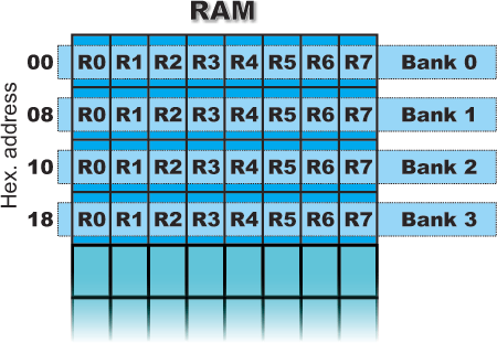
RS0, RS1 - Register bank select bits. These two bits are used to select one of four register banks of RAM. By setting and clearing these bits, registers R0-R7 are stored in one of four banks of RAM.
PSW register is one of the most important SFRs. It contains several status bits that reflect the current state of the CPU. Besides, this register contains Carry bit, Auxiliary Carry, two register bank select bits, Overflow flag, parity bit and user-definable status flag.
P - Parity bit. If a number stored in the accumulator is even then this bit will be automatically set (1), otherwise it will be cleared (0). It is mainly used during data transmit and receive via serial communication.
- Bit 1. This bit is intended to be used in the future versions of microcontrollers.
OV Overflow occurs when the result of an arithmetical operation is larger than 255 and cannot be stored in one register. Overflow condition causes the OV bit to be set (1). Otherwise, it will be cleared (0).
RS0, RS1 - Register bank select bits. These two bits are used to select one of four register banks of RAM. By setting and clearing these bits, registers R0-R7 are stored in one of four banks of RAM.
| RS1 | RS2 | SPACE IN RAM |
|---|---|---|
| 0 | 0 | Bank0 00h-07h |
| 0 | 1 | Bank1 08h-0Fh |
| 1 | 0 | Bank2 10h-17h |
| 1 | 1 | Bank3 18h-1Fh |
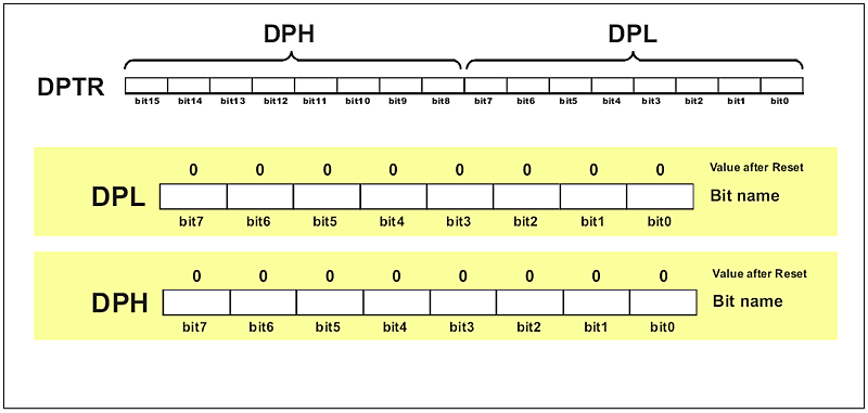
 A value stored in the Stack Pointer points to the first free stack address and permits stack availability. Stack pushes increment the value in the Stack Pointer by 1. Likewise, stack pops decrement its value by 1. Upon any reset and power-on, the value 7 is stored in the Stack Pointer, which means that the space of RAM reserved for the stack starts at this location. If another value is written to this register, the entire Stack is moved to the new memory location.
 If neither external memory nor serial communication system are used then 4 ports with in total of 32 input/output pins are available for connection to peripheral environment. Each bit within these ports affects the state and performance of appropriate pin of the microcontroller. Thus, bit logic state is reflected on appropriate pin as a voltage (0 or 5 V) and vice versa, voltage on a pin reflects the state of appropriate port bit.
As mentioned, port bit state affects performance of port pins, i.e. whether they will be configured as inputs or outputs. If a bit is cleared (0), the appropriate pin will be configured as an output, while if it is set (1), the appropriate pin will be configured as an input. Upon reset and power-on, all port bits are set (1), which means that all appropriate pins will be configured as inputs.
If neither external memory nor serial communication system are used then 4 ports with in total of 32 input/output pins are available for connection to peripheral environment. Each bit within these ports affects the state and performance of appropriate pin of the microcontroller. Thus, bit logic state is reflected on appropriate pin as a voltage (0 or 5 V) and vice versa, voltage on a pin reflects the state of appropriate port bit.
As mentioned, port bit state affects performance of port pins, i.e. whether they will be configured as inputs or outputs. If a bit is cleared (0), the appropriate pin will be configured as an output, while if it is set (1), the appropriate pin will be configured as an input. Upon reset and power-on, all port bits are set (1), which means that all appropriate pins will be configured as inputs.


